- 您現(xiàn)在的位置:買賣IC網(wǎng) > PDF目錄384755 > MT48LC64M8A2 (Micron Technology, Inc.) SYNCHRONOUS DRAM PDF資料下載
參數(shù)資料
| 型號(hào): | MT48LC64M8A2 |
| 廠商: | Micron Technology, Inc. |
| 英文描述: | SYNCHRONOUS DRAM |
| 中文描述: | 同步DRAM |
| 文件頁(yè)數(shù): | 19/55頁(yè) |
| 文件大小: | 1828K |
| 代理商: | MT48LC64M8A2 |
第1頁(yè)第2頁(yè)第3頁(yè)第4頁(yè)第5頁(yè)第6頁(yè)第7頁(yè)第8頁(yè)第9頁(yè)第10頁(yè)第11頁(yè)第12頁(yè)第13頁(yè)第14頁(yè)第15頁(yè)第16頁(yè)第17頁(yè)第18頁(yè)當(dāng)前第19頁(yè)第20頁(yè)第21頁(yè)第22頁(yè)第23頁(yè)第24頁(yè)第25頁(yè)第26頁(yè)第27頁(yè)第28頁(yè)第29頁(yè)第30頁(yè)第31頁(yè)第32頁(yè)第33頁(yè)第34頁(yè)第35頁(yè)第36頁(yè)第37頁(yè)第38頁(yè)第39頁(yè)第40頁(yè)第41頁(yè)第42頁(yè)第43頁(yè)第44頁(yè)第45頁(yè)第46頁(yè)第47頁(yè)第48頁(yè)第49頁(yè)第50頁(yè)第51頁(yè)第52頁(yè)第53頁(yè)第54頁(yè)第55頁(yè)
19
512Mb: x4, x8, x16 SDRAM
512MSDRAM_D.p65
–
Rev. D; Pub 1/02
Micron Technology, Inc., reserves the right to change products or specifications without notice.
2000, Micron Technology, Inc.
512Mb: x4, x8, x16
SDRAM
ADVANCE
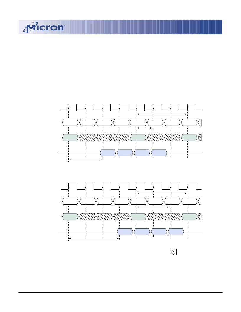
Figure 11
READ to PRECHARGE
A fixed-length READ burst may be followed by, or
truncated with, a PRECHARGE command to the same
bank (provided that auto precharge was not activated),
and a full-page burst may be truncated with a
PRECHARGE command to the same bank. The
PRECHARGE command should be issued
x
cycles before
the clock edge at which the last desired data element is
valid, where
x
equals the CAS latency minus one. This is
shown in Figure 11 for each possible CAS latency; data
element
n
+ 3 is either the last of a burst of four or the last
desired of a longer burst. Following the PRECHARGE
command, a subsequent command to the same bank
cannot be issued until
t
RP is met. Note that part of the row
precharge time is hidden during the access of the last
data element(s).
In the case of a fixed-length burst being executed to
completion, a PRECHARGE command issued at the opti-
mum time (as described above) provides the same op-
DON
’
T CARE
CLK
DQ
D
OUT
n
T2
T1
T4
T3
T6
T5
T0
COMMAND
ADDRESS
READ
NOP
NOP
NOP
NOP
NOP
D
OUT
n
+ 1
D
OUT
n
+ 2
D
OUT
n
+ 3
PRECHARGE
ACTIVE
tRP
T7
NOTE:
DQM is LOW.
CLK
DQ
D
OUT
n
T2
T1
T4
T3
T6
T5
T0
COMMAND
ADDRESS
READ
NOP
NOP
NOP
NOP
NOP
D
OUT
n
+ 1
D
OUT
n
+ 2
D
OUT
n
+ 3
PRECHARGE
ACTIVE
tRP
T7
X
= 1 cycle
CAS Latency = 2
CAS Latency = 3
X
= 2 cycles
BANK
a
,
COL
n
BANK
a
,
ROW
BANK
(
a
or all)
BANK
a
,
COL
n
BANK
a
,
ROW
BANK
(
a
or all)
相關(guān)PDF資料 |
PDF描述 |
|---|---|
| MT48LC32M16A2 | SYNCHRONOUS DRAM |
| MT48LC8M16A2FB-75LIT | SYNCHRONOUS DRAM |
| MT48LC8M16A2FB-7E | SYNCHRONOUS DRAM |
| MT48LC8M16A2FB-7EIT | SYNCHRONOUS DRAM |
| MT48LC8M16A2FB-7EL | SYNCHRONOUS DRAM |
相關(guān)代理商/技術(shù)參數(shù) |
參數(shù)描述 |
|---|
發(fā)布緊急采購(gòu),3分鐘左右您將得到回復(fù)。