- 您現(xiàn)在的位置:買賣IC網(wǎng) > PDF目錄384755 > MT48LC32M16A2 (Micron Technology, Inc.) SYNCHRONOUS DRAM PDF資料下載
參數(shù)資料
| 型號: | MT48LC32M16A2 |
| 廠商: | Micron Technology, Inc. |
| 英文描述: | SYNCHRONOUS DRAM |
| 中文描述: | 同步DRAM |
| 文件頁數(shù): | 21/55頁 |
| 文件大小: | 1828K |
| 代理商: | MT48LC32M16A2 |
第1頁第2頁第3頁第4頁第5頁第6頁第7頁第8頁第9頁第10頁第11頁第12頁第13頁第14頁第15頁第16頁第17頁第18頁第19頁第20頁當前第21頁第22頁第23頁第24頁第25頁第26頁第27頁第28頁第29頁第30頁第31頁第32頁第33頁第34頁第35頁第36頁第37頁第38頁第39頁第40頁第41頁第42頁第43頁第44頁第45頁第46頁第47頁第48頁第49頁第50頁第51頁第52頁第53頁第54頁第55頁
21
512Mb: x4, x8, x16 SDRAM
512MSDRAM_D.p65
–
Rev. D; Pub 1/02
Micron Technology, Inc., reserves the right to change products or specifications without notice.
2000, Micron Technology, Inc.
512Mb: x4, x8, x16
SDRAM
ADVANCE
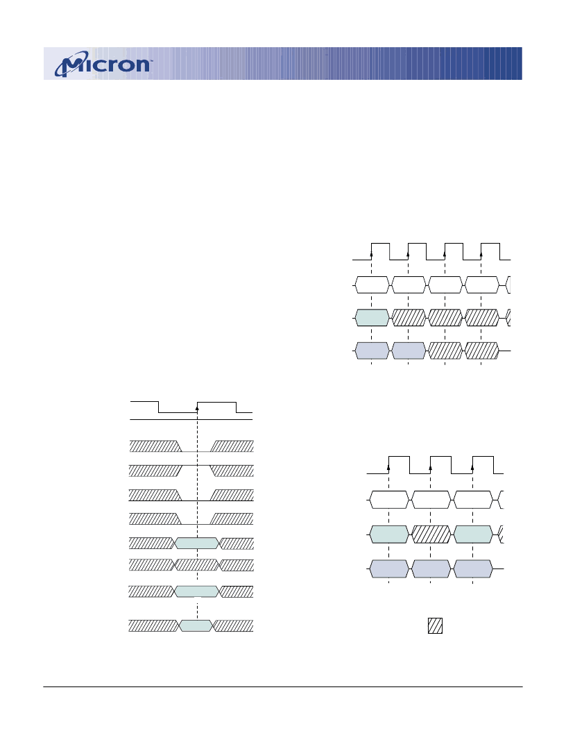
WRITEs
WRITE bursts are initiated with a WRITE command,
as shown in Figure 13.
The starting column and bank addresses are provided
with the WRITE command, and auto precharge is either
enabled or disabled for that access. If auto precharge is
enabled, the row being accessed is precharged at the
completion of the burst. For the generic WRITE com-
mands used in the following illustrations, auto precharge
is disabled.
During WRITE bursts, the first valid data-in element
will be registered coincident with the WRITE command.
Subsequent data elements will be registered on each
successive positive clock edge. Upon completion of a
fixed-length burst, assuming no other commands have
been initiated, the DQs will remain High-Z and any addi-
tional input data will be ignored (see Figure 14). A full-
page burst will continue until terminated. (At the end of
the page, it will wrap to the start address and continue.)
Data for any WRITE burst may be truncated with a
subsequent WRITE command, and data for a fixed-length
WRITE burst may be immediately followed by data for a
WRITE command. The new WRITE command can be
issued on any clock following the previous WRITE com-
mand, and the data provided coincident with the new
command applies to the new command. An example is
Figure 15
WRITE to WRITE
shown in Figure 15. Data
n
+ 1 is either the last of a burst
of two or the last desired of a longer burst. The 512Mb
SDRAM uses a pipelined architecture and therefore does
not require the 2
n
rule associated with a prefetch archi-
tecture. A WRITE command can be initiated on any clock
cycle following a previous WRITE command. Full-speed
random write accesses within a page can be performed to
the same bank, as shown in Figure 16, or each subsequent
WRITE may be performed to a different bank.
CLK
DQ
D
IN
n
T2
T1
T3
T0
COMMAND
ADDRESS
NOP
NOP
WRITE
D
IN
n
+ 1
NOP
BANK,
COL
n
NOTE
B
t l
th
Figure 14
WRITE Burst
2 DQM i LOW
CLK
DQ
T2
T1
T0
COMMAND
ADDRESS
NOP
WRITE
WRITE
BANK,
COL
n
BANK,
COL
b
D
IN
n
D
IN
n
+ 1
D
IN
b
NOTE:
DQM is LOW.
Each WRITE
command may be to any bank.
DON
’
T CARE
Figure 13
WRITE Command
CS#
WE#
CAS#
RAS#
CKE
CLK
COLUMN
A10
HIGH
ENABLE AUTO PRECHARGE
DISABLE AUTO PRECHARGE
A0-A9, A11, A12: x4
A0-A9, A11: x8
A0-A9: x16
A12: x4
A11, A12: x8
A9, A11, A12: x16
BA0, BA, 1
ABANK
相關PDF資料 |
PDF描述 |
|---|---|
| MT48LC8M16A2FB-75LIT | SYNCHRONOUS DRAM |
| MT48LC8M16A2FB-7E | SYNCHRONOUS DRAM |
| MT48LC8M16A2FB-7EIT | SYNCHRONOUS DRAM |
| MT48LC8M16A2FB-7EL | SYNCHRONOUS DRAM |
| MT48LC8M16A2FB-7ELIT | SYNCHRONOUS DRAM |
相關代理商/技術參數(shù) |
參數(shù)描述 |
|---|---|
| MT48LC32M16A2-75ITC | 制造商:Micron Technology Inc 功能描述: |
| MT48LC32M16A2P-75 | 制造商:Micron Technology Inc 功能描述: |
| MT48LC32M16A2P-75 C TR | 制造商:Micron Technology Inc 功能描述:DRAM Chip SDRAM 512M-Bit 32Mx16 3.3V 54-Pin TSOP-II T/R 制造商:Micron Technology 功能描述:DRAM Chip SDRAM 512M-Bit 32Mx16 3.3V 54-Pin TSOP-II T/R |
發(fā)布緊急采購,3分鐘左右您將得到回復。