- 您現(xiàn)在的位置:買賣IC網(wǎng) > PDF目錄45401 > MSP430F5437IPNR (TEXAS INSTRUMENTS INC) 16-BIT, FLASH, 25 MHz, RISC MICROCONTROLLER, PQFP80 PDF資料下載
參數(shù)資料
| 型號: | MSP430F5437IPNR |
| 廠商: | TEXAS INSTRUMENTS INC |
| 元件分類: | 微控制器/微處理器 |
| 英文描述: | 16-BIT, FLASH, 25 MHz, RISC MICROCONTROLLER, PQFP80 |
| 封裝: | GREEN, PLASTIC, LQFP-80 |
| 文件頁數(shù): | 55/99頁 |
| 文件大?。?/td> | 985K |
| 代理商: | MSP430F5437IPNR |
第1頁第2頁第3頁第4頁第5頁第6頁第7頁第8頁第9頁第10頁第11頁第12頁第13頁第14頁第15頁第16頁第17頁第18頁第19頁第20頁第21頁第22頁第23頁第24頁第25頁第26頁第27頁第28頁第29頁第30頁第31頁第32頁第33頁第34頁第35頁第36頁第37頁第38頁第39頁第40頁第41頁第42頁第43頁第44頁第45頁第46頁第47頁第48頁第49頁第50頁第51頁第52頁第53頁第54頁當(dāng)前第55頁第56頁第57頁第58頁第59頁第60頁第61頁第62頁第63頁第64頁第65頁第66頁第67頁第68頁第69頁第70頁第71頁第72頁第73頁第74頁第75頁第76頁第77頁第78頁第79頁第80頁第81頁第82頁第83頁第84頁第85頁第86頁第87頁第88頁第89頁第90頁第91頁第92頁第93頁第94頁第95頁第96頁第97頁第98頁第99頁
MSP430F543x, MSP430F541x
www.ti.com
SLAS612C – AUGUST 2009 – REVISED MARCH 2010
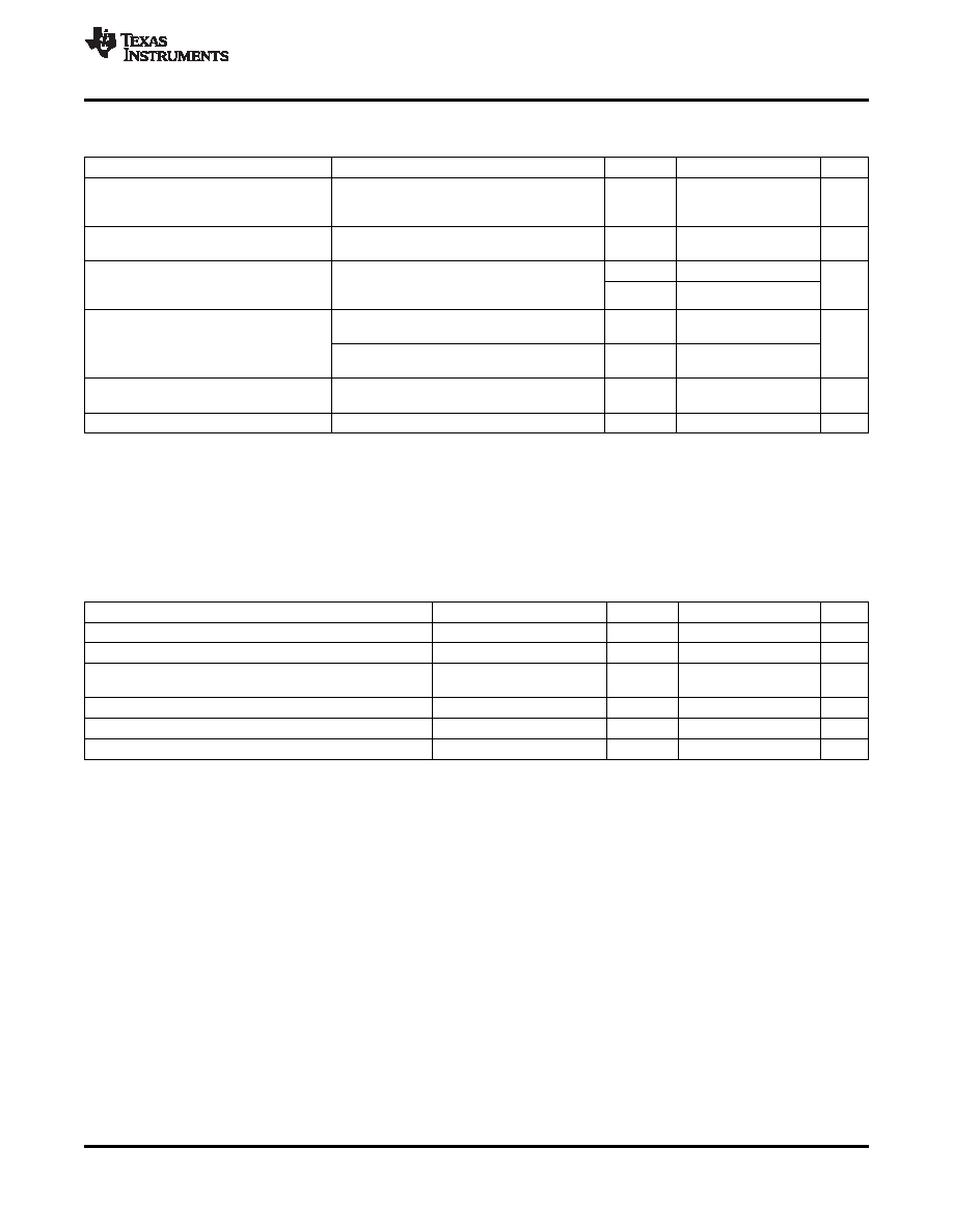
12-Bit ADC, Power Supply and Input Range Conditions
over recommended ranges of supply voltage and operating free-air temperature (unless otherwise noted)
(1)
PARAMETER
TEST CONDITIONS
VCC
MIN
TYP
MAX
UNIT
AVCC and DVCC are connected together,
AVCC
Analog supply voltage
AVSS and DVSS are connected together,
2.2
3.6
V
V(AVSS) = V(DVSS) = 0 V
All ADC12 pins: P6.0 to P6.7, P7.4 to P7.7,
V(Ax)
Analog input voltage range(2)
0
AVCC
V
P5.0, and P5.1 terminals
fADC12CLK = 5.0 MHz, ADC12ON = 1,
2.2 V
125
155
Operating supply current into
IADC12_A
REFON = 0, SHT0 = 0, SHT1 = 0,
A
AVCC terminal
(3)
3 V
150
220
ADC12DIV = 0
ADC12ON = 0,
3 V
150
190
REFON = 1, REF2_5V = 1
Operating supply current into
IREF+
A
AVCC terminal
(4)
ADC12ON = 0,
2.2 V/3 V
150
180
REFON = 1, REF2_5V = 0
Only one terminal Ax can be selected at one
CI
Input capacitance
2.2 V
20
25
pF
time
RI
Input MUX ON resistance
0 V
≤ VAx ≤ AVCC
10
200
1900
(1)
The leakage current is specified by the digital I/O input leakage.
(2)
The analog input voltage range must be within the selected reference voltage range VR+ to VR– for valid conversion results. If the
reference voltage is supplied by an external source or if the internal reference voltage is used and REFOUT = 1, then decoupling
capacitors are required. See 12-Bit ADC, External Reference and 12-Bit ADC, Built-In Reference.
(3)
The internal reference supply current is not included in current consumption parameter IADC12.
(4)
The internal reference current is supplied via terminal AVCC. Consumption is independent of the ADC12ON control bit, unless a
conversion is active. The REFON bit enables to settle the built-in reference before starting an A/D conversion. No external load.
12-Bit ADC, External Reference
over recommended ranges of supply voltage and operating free-air temperature (unless otherwise noted)
(1)
PARAMETER
TEST CONDITIONS
VCC
MIN
TYP
MAX
UNIT
VeREF+
Positive external reference voltage input
VeREF+ > VREF–/VeREF–
(2)
1.4
AVCC
V
VREF–/VeREF–
Negative external reference voltage input
VeREF+ > VREF–/VeREF–
(3)
0
1.2
V
(VeREF+ –
Differential external reference voltage
VeREF+ > VREF–/VeREF–
(4)
1.4
AVCC
V
VREF–/VeREF–)
input
IVeREF+
Static input current
0 V
≤ VeREF+ ≤ VAVCC
2.2 V/3 V
±1
A
IVREF–/VeREF–
Static input current
0 V
≤ VeREF– ≤ VAVCC
2.2 V/3 V
±1
A
CVREF+/-
Capacitance at VREF+/- terminal
(5)10
F
(1)
The external reference is used during conversion to charge and discharge the capacitance array. The input capacitance, Ci, is also the
dynamic load for an external reference during conversion. The dynamic impedance of the reference supply should follow the
recommendations on analog-source impedance to allow the charge to settle for 12-bit accuracy.
(2)
The accuracy limits the minimum positive external reference voltage. Lower reference voltage levels may be applied with reduced
accuracy requirements.
(3)
The accuracy limits the maximum negative external reference voltage. Higher reference voltage levels may be applied with reduced
accuracy requirements.
(4)
The accuracy limits minimum external differential reference voltage. Lower differential reference voltage levels may be applied with
reduced accuracy requirements.
(5)
Two decoupling capacitors, 10F and 100nF, should be connected to VREF to decouple the dynamic current required for an external
reference source if it is used for the ADC12_A. See also the MSP430x5xx Family User's Guide (SLAU208).
Copyright 2009–2010, Texas Instruments Incorporated
59
相關(guān)PDF資料 |
PDF描述 |
|---|---|
| MSP430F5438AIPZ | 16-BIT, FLASH, 25 MHz, RISC MICROCONTROLLER, PQFP100 |
| MSP430F5435AIPNR | 16-BIT, FLASH, 25 MHz, RISC MICROCONTROLLER, PQFP80 |
| MSP430F5419AIZQW | 16-BIT, FLASH, 25 MHz, RISC MICROCONTROLLER, PBGA113 |
| MSP430F5438AIZQWR | 16-BIT, FLASH, 25 MHz, RISC MICROCONTROLLER, PBGA113 |
| MSP430F5436AIPZ | 16-BIT, FLASH, 25 MHz, RISC MICROCONTROLLER, PQFP100 |
相關(guān)代理商/技術(shù)參數(shù) |
參數(shù)描述 |
|---|---|
| MSP430F5438ACY | 制造商:Texas Instruments 功能描述:IC MCU 16BIT 256KB FLASH DIE 制造商:Texas Instruments 功能描述:MSP430F5438A - DIE SALES |
| MSP430F5438ACYS | 制造商:Texas Instruments 功能描述:IC MCU 16BIT 256KB FLASH DIE 制造商:Texas Instruments 功能描述:Ultra low power Micro Controller - Wafer |
| MSP430F5438AIPZ | 功能描述:16位微控制器 - MCU 16B Ultra-Low-Pwr Microcontroller RoHS:否 制造商:Texas Instruments 核心:RISC 處理器系列:MSP430FR572x 數(shù)據(jù)總線寬度:16 bit 最大時鐘頻率:24 MHz 程序存儲器大小:8 KB 數(shù)據(jù) RAM 大小:1 KB 片上 ADC:Yes 工作電源電壓:2 V to 3.6 V 工作溫度范圍:- 40 C to + 85 C 封裝 / 箱體:VQFN-40 安裝風(fēng)格:SMD/SMT |
| MSP430F5438AIPZR | 功能描述:16位微控制器 - MCU 16B Ultra-Low-Pwr Microcontroller RoHS:否 制造商:Texas Instruments 核心:RISC 處理器系列:MSP430FR572x 數(shù)據(jù)總線寬度:16 bit 最大時鐘頻率:24 MHz 程序存儲器大小:8 KB 數(shù)據(jù) RAM 大小:1 KB 片上 ADC:Yes 工作電源電壓:2 V to 3.6 V 工作溫度范圍:- 40 C to + 85 C 封裝 / 箱體:VQFN-40 安裝風(fēng)格:SMD/SMT |
| MSP430F5438AIZQW | 制造商:Texas Instruments 功能描述:16-BIT ULTRA-LOW-POWER MICROCONTROLLER, 256KB FLASH, - Tape and Reel |
發(fā)布緊急采購,3分鐘左右您將得到回復(fù)。