- 您現(xiàn)在的位置:買賣IC網(wǎng) > PDF目錄382345 > MPC9772 (Motorola, Inc.) 3.3V 1:12 LVCMOS PLL Clock Generator PDF資料下載
參數(shù)資料
| 型號: | MPC9772 |
| 廠商: | Motorola, Inc. |
| 英文描述: | 3.3V 1:12 LVCMOS PLL Clock Generator |
| 中文描述: | 3.3 1:12的LVCMOS PLL時鐘發(fā)生器 |
| 文件頁數(shù): | 11/16頁 |
| 文件大小: | 238K |
| 代理商: | MPC9772 |
MPC9772
TIMING SOLUTIONS
11
MOTOROLA
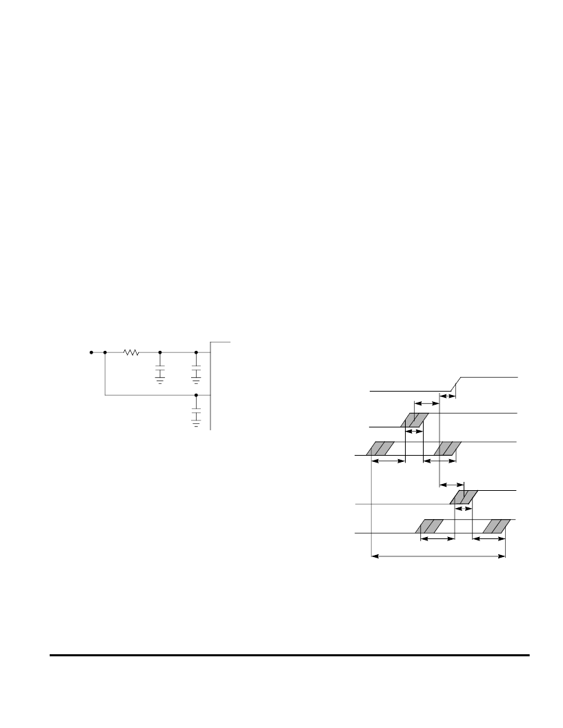
Power Supply Filtering
The MPC9772 is a mixed analog/digital product. Its analog
circuitry is naturally susceptible to random noise, especially if
this noise is seen on the power supply pins. Random noise on
the V
CC_PLL
power supply impacts the device characteristics,
for instance I/O jitter. The MPC9772 provides separate power
supplies for the output buffers (V
CC
) and the phase-locked loop
(V
CC_PLL
) of the device. The purpose of this design technique
is to isolate the high switching noise digital outputs from the
relatively sensitive internal analog phase-locked loop. In a
digital system environment where it is more difficult to minimize
noise on the power supplies a second level of isolation may be
required. The simple but effective form of isolation is a power
supply filter on the V
CCA_PLL
pin for the MPC9772. Figure 7
illustrates a typical power supply filter scheme. The MPC9772
frequency and phase stability is most susceptible to noise with
spectral content in the 100kHz to 20MHz range. Therefore the
filter should be designed to target this range. The key
parameter that needs to be met in the final filter design is the DC
voltage drop across the series filter resistor R
F
. From the data
sheet the I
CC_PLL
current (the current sourced through
the V
CC_PLL
pin) is typically 3 mA (5 mA maximum), assuming
that a minimum of 3.0V must be maintained on the V
CC_PLL
pin.
The resistor R
F
shown in Figure 7 must have a resistance of
5-10
to meet the voltage drop criteria.
The minimum values for R
F
and the filter capacitor C
F
are
defined by the required filter characteristics: the RC filter should
provide an attenuation greater than 40 dB for noise whose
spectral content is above 100 kHz. In the example RC filter
shown in Figure 7. “V
CC_PLL
Power Supply Filter”, the filter
cut-off frequency is around 4.5 kHz and the noise attenuation at
100 kHz is better than 42 dB.
As the noise frequency crosses the series resonant point of
an individual capacitor its overall impedance begins to look
inductive and thus increases with increasing frequency. The
parallel capacitor combination shown ensures that a low
impedance path to ground exists for frequencies well above the
bandwidth of the PLL. Although the MPC9772 has several
design features to minimize the susceptibility to power supply
noise (isolated power and grounds and fully differential PLL)
there still may be applications in which overall performance is
being degraded due to system power supply noise. The power
supply filter schemes discussed in this section should be
adequate to eliminate power supply noise related problems in
most designs.
Using the MPC9772 in Zero-Delay Applications
Nested clock trees are typical applications for the MPC9772.
Designs using the MPC9772 as LVCMOS PLL fanout buffer
with zero insertion delay will show significantly lower clock skew
than clock distributions developed from CMOS fanout buffers.
The external feedback option of the MPC9772 clock driver
allows for its use as a zero delay buffer. The PLL aligns the
feedback clock output edge with the clock input reference edge
resulting a near zero delay through the device (the propagation
delay through the device is virtually eliminated). The maximum
insertion delay of the device in zero-delay applications is
measured between the reference clock input and any output.
This effective delay consists of the static phase offset, I/O jitter
(phase or long-term jitter), feedback path delay and the
output-to-output skew error relative to the feedback output.
Calculation of Part-to-Part Skew
The MPC9772 zero delay buffer supports applications where
critical clock signal timing can be maintained across several
devices. If the reference clock inputs of two or more MPC9772
are connected together, the maximum overall timing uncertainty
from the common CCLKx input to any output is:
t
SK(PP)
= t
(
)
+ t
SK(O)
+ t
PD, LINE(FB)
+ t
JIT(
)
CF
This maximum timing uncertainty consist of 4 components:
static phase offset, output skew, feedback board trace delay
and I/O (phase) jitter:
Due to the statistical nature of I/O jitter a RMS value (1
σ
) is
specified. I/O jitter numbers for other confidence factors (CF)
can be derived from Table 12.
Figure 7. V
CC_PLL
Power Supply Filter
V
CC_PLL
V
CC
MPC9772
10 nF
R
F
= 5–10
C
F
33...100 nF
R
F
V
CC
C
F
= 22
μ
F
Figure 8. MPC9772 Maximum
Device-to-Device Skew
t
PD,LINE(FB)
t
JIT(
)
+
t
SK(O)
–t
(
)
+t
(
)
t
JIT(
)
+
t
SK(O)
t
SK(PP)
Max. skew
CCLK
Common
QFB
Device 1
Any Q
Device 1
QFB
Device2
Any Q
Device 2
相關(guān)PDF資料 |
PDF描述 |
|---|---|
| MPC9893 | Low Voltage PLL Intelligent Dynamic Clock (IDCS) Switch |
| MPC99J93 | Intelligent Dynamic Clock Switch (IDCS) PLL Clock Driver |
| MPD-425V | 250W DC-DC POWER SUPPLY INPUT RANGE: 40~57VDC |
| MPE-902M | SWITCHING POWER SUPPLY |
| MPF102G | JFET VHF Amplifier |
相關(guān)代理商/技術(shù)參數(shù) |
參數(shù)描述 |
|---|---|
| MPC9772AE | 功能描述:鎖相環(huán) - PLL 2.5 3.3V 250MHz Clock Generator RoHS:否 制造商:Silicon Labs 類型:PLL Clock Multiplier 電路數(shù)量:1 最大輸入頻率:710 MHz 最小輸入頻率:0.002 MHz 輸出頻率范圍:0.002 MHz to 808 MHz 電源電壓-最大:3.63 V 電源電壓-最小:1.71 V 最大工作溫度:+ 85 C 最小工作溫度:- 40 C 封裝 / 箱體:QFN-36 封裝:Tray |
| MPC9772AER2 | 功能描述:時鐘發(fā)生器及支持產(chǎn)品 FSL 1-12 LVCMOS PLL Clock Generator, xta RoHS:否 制造商:Silicon Labs 類型:Clock Generators 最大輸入頻率:14.318 MHz 最大輸出頻率:166 MHz 輸出端數(shù)量:16 占空比 - 最大:55 % 工作電源電壓:3.3 V 工作電源電流:1 mA 最大工作溫度:+ 85 C 安裝風(fēng)格:SMD/SMT 封裝 / 箱體:QFN-56 |
| MPC9772FA | 功能描述:鎖相環(huán) - PLL 3.3V 240MHz Clock Generator RoHS:否 制造商:Silicon Labs 類型:PLL Clock Multiplier 電路數(shù)量:1 最大輸入頻率:710 MHz 最小輸入頻率:0.002 MHz 輸出頻率范圍:0.002 MHz to 808 MHz 電源電壓-最大:3.63 V 電源電壓-最小:1.71 V 最大工作溫度:+ 85 C 最小工作溫度:- 40 C 封裝 / 箱體:QFN-36 封裝:Tray |
| MPC9772FAR2 | 功能描述:時鐘發(fā)生器及支持產(chǎn)品 FSL 1-12 LVCMOS PLL Clock Generator, xta RoHS:否 制造商:Silicon Labs 類型:Clock Generators 最大輸入頻率:14.318 MHz 最大輸出頻率:166 MHz 輸出端數(shù)量:16 占空比 - 最大:55 % 工作電源電壓:3.3 V 工作電源電流:1 mA 最大工作溫度:+ 85 C 安裝風(fēng)格:SMD/SMT 封裝 / 箱體:QFN-56 |
| MPC9773 | 制造商:FREESCALE 制造商全稱:Freescale Semiconductor, Inc 功能描述:3.3 V 1:12 LVCMOS PLL Clock Generator |
發(fā)布緊急采購,3分鐘左右您將得到回復(fù)。