- 您現(xiàn)在的位置:買賣IC網(wǎng) > PDF目錄1955 > MPC8349ECZUAJFB (Freescale Semiconductor)IC MPU POWERQUICC II PRO 672TBGA PDF資料下載
參數(shù)資料
| 型號: | MPC8349ECZUAJFB |
| 廠商: | Freescale Semiconductor |
| 文件頁數(shù): | 8/87頁 |
| 文件大小: | 0K |
| 描述: | IC MPU POWERQUICC II PRO 672TBGA |
| 標準包裝: | 24 |
| 系列: | MPC83xx |
| 處理器類型: | 32-位 MPC83xx PowerQUICC II Pro |
| 速度: | 533MHz |
| 電壓: | 1.2V |
| 安裝類型: | 表面貼裝 |
| 封裝/外殼: | 672-LBGA |
| 供應商設備封裝: | 672-TBGA(35x35) |
| 包裝: | 托盤 |
| 配用: | MPC8349E-MITX-GP-ND - KIT REFERENCE PLATFORM MPC8349E MPC8349E-MITXE-ND - BOARD REFERENCE FOR MPC8349 MPC8349EA-MDS-PB-ND - KIT MODULAR DEV SYSTEM MPC8349E |
第1頁第2頁第3頁第4頁第5頁第6頁第7頁當前第8頁第9頁第10頁第11頁第12頁第13頁第14頁第15頁第16頁第17頁第18頁第19頁第20頁第21頁第22頁第23頁第24頁第25頁第26頁第27頁第28頁第29頁第30頁第31頁第32頁第33頁第34頁第35頁第36頁第37頁第38頁第39頁第40頁第41頁第42頁第43頁第44頁第45頁第46頁第47頁第48頁第49頁第50頁第51頁第52頁第53頁第54頁第55頁第56頁第57頁第58頁第59頁第60頁第61頁第62頁第63頁第64頁第65頁第66頁第67頁第68頁第69頁第70頁第71頁第72頁第73頁第74頁第75頁第76頁第77頁第78頁第79頁第80頁第81頁第82頁第83頁第84頁第85頁第86頁第87頁
MPC8349EA PowerQUICC II Pro Integrated Host Processor Hardware Specifications, Rev. 13
16
Freescale Semiconductor
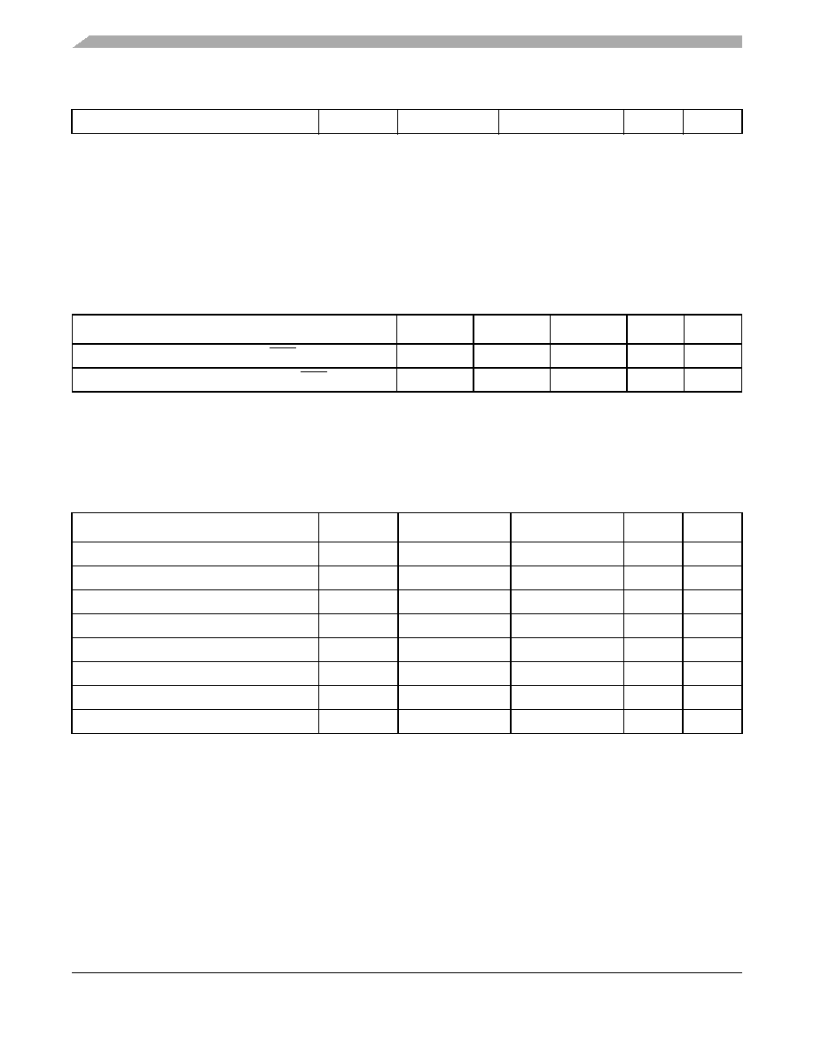
DDR and DDR2 SDRAM
Table 14 provides the recommended operating conditions for the DDR SDRAM component(s) when
GVDD(typ) = 2.5 V.
Output low current (VOUT = 0.280 V)
IOL
13.4
—
mA
—
Notes:
1. GVDD is expected to be within 50 mV of the DRAM GVDD at all times.
2. MVREF is expected to equal 0.5 × GVDD, and to track GVDD DC variations as measured at the receiver. Peak-to-peak noise
on MVREF cannot exceed ±2% of the DC value.
3. VTT is not applied directly to the device. It is the supply to which far end signal termination is made and is expected to equal
MVREF. This rail should track variations in the DC level of MVREF.
4. Output leakage is measured with all outputs disabled, 0 V
≤ V
OUT ≤ GVDD.
Table 13. DDR2 SDRAM Capacitance for GVDD(typ) = 1.8 V
Parameter/Condition
Symbol
Min
Max
Unit
Notes
Input/output capacitance: DQ, DQS, DQS
CIO
68
pF
1
Delta input/output capacitance: DQ, DQS, DQS
CDIO
—0.5
pF
1
Note:
1. This parameter is sampled. GVDD = 1.8 V ± 0.090 V, f = 1 MHz, TA = 25°C, VOUT = GVDD/2, VOUT (peak-to-peak) = 0.2 V.
Table 14. DDR SDRAM DC Electrical Characteristics for GVDD(typ) = 2.5 V
Parameter/Condition
Symbol
Min
Max
Unit
Notes
I/O supply voltage
GVDD
2.375
2.625
V
1
I/O reference voltage
MVREF
0.49
× GV
DD
0.51
× GV
DD
V2
I/O termination voltage
VTT
MVREF –0.04
MVREF +0.04
V
3
Input high voltage
VIH
MVREF +0.18
GVDD +0.3
V
—
Input low voltage
VIL
–0.3
MVREF –0.18
V
—
Output leakage current
IOZ
–9.9
μA4
Output high current (VOUT = 1.95 V)
IOH
–15.2
—
mA
—
Output low current (VOUT = 0.35 V)
IOL
15.2
—
mA
—
Notes:
1. GVDD is expected to be within 50 mV of the DRAM GVDD at all times.
2. MVREF is expected to be equal to 0.5 × GVDD, and to track GVDD DC variations as measured at the receiver. Peak-to-peak
noise on MVREF may not exceed ±2% of the DC value.
3. VTT is not applied directly to the device. It is the supply to which far end signal termination is made and is expected to be
equal to MVREF. This rail should track variations in the DC level of MVREF.
4. Output leakage is measured with all outputs disabled, 0 V
≤ V
OUT ≤ GVDD.
Table 12. DDR2 SDRAM DC Electrical Characteristics for GVDD(typ) = 1.8 V (continued)
相關PDF資料 |
PDF描述 |
|---|---|
| MPC8358ECZUADDE | IC MPU PWRQUICC II 740-TBGA |
| MPC8358EVVAGDG | IC MPU POWERQUICC II 740-TBGA |
| MPC8360EVVAJDGA | IC MPU POWERQUICC II PRO 740TBGA |
| MPC8377CVRANGA | MPU POWERQUICC II 800MHZ 689PBGA |
| MPC8377EVRANG | MPU POWERQUICC II PRO 689-PBGA |
相關代理商/技術參數(shù) |
參數(shù)描述 |
|---|---|
| MPC8349ECZUALDB | 制造商:FREESCALE 制造商全稱:Freescale Semiconductor, Inc 功能描述:Integrated Host Processor Hardware Specifications |
| MPC8349ECZUALFB | 制造商:FREESCALE 制造商全稱:Freescale Semiconductor, Inc 功能描述:Integrated Host Processor Hardware Specifications |
| MPC8349E-MDS | 功能描述:開發(fā)板和工具包 - 其他處理器 KIT FOR MPC8349E BDS RoHS:否 制造商:Freescale Semiconductor 產(chǎn)品:Development Systems 工具用于評估:P3041 核心:e500mc 接口類型:I2C, SPI, USB 工作電源電壓: |
| MPC8349E-MDS-PB | 功能描述:開發(fā)板和工具包 - 其他處理器 PROCESSR BD MPC8349E RoHS:否 制造商:Freescale Semiconductor 產(chǎn)品:Development Systems 工具用于評估:P3041 核心:e500mc 接口類型:I2C, SPI, USB 工作電源電壓: |
| MPC8349E-MDS-PBE | 功能描述:開發(fā)板和工具包 - 其他處理器 MPC8349E FAMILY ADS RoHS:否 制造商:Freescale Semiconductor 產(chǎn)品:Development Systems 工具用于評估:P3041 核心:e500mc 接口類型:I2C, SPI, USB 工作電源電壓: |
發(fā)布緊急采購,3分鐘左右您將得到回復。