- 您現(xiàn)在的位置:買賣IC網(wǎng) > PDF目錄369923 > MPC106 (Motorola, Inc.) 32-Bit Microprocessor(32位微處理器) PDF資料下載
參數(shù)資料
| 型號(hào): | MPC106 |
| 廠商: | Motorola, Inc. |
| 英文描述: | 32-Bit Microprocessor(32位微處理器) |
| 中文描述: | 32位微處理器(32位微處理器) |
| 文件頁數(shù): | 127/398頁 |
| 文件大?。?/td> | 1112K |
| 代理商: | MPC106 |
第1頁第2頁第3頁第4頁第5頁第6頁第7頁第8頁第9頁第10頁第11頁第12頁第13頁第14頁第15頁第16頁第17頁第18頁第19頁第20頁第21頁第22頁第23頁第24頁第25頁第26頁第27頁第28頁第29頁第30頁第31頁第32頁第33頁第34頁第35頁第36頁第37頁第38頁第39頁第40頁第41頁第42頁第43頁第44頁第45頁第46頁第47頁第48頁第49頁第50頁第51頁第52頁第53頁第54頁第55頁第56頁第57頁第58頁第59頁第60頁第61頁第62頁第63頁第64頁第65頁第66頁第67頁第68頁第69頁第70頁第71頁第72頁第73頁第74頁第75頁第76頁第77頁第78頁第79頁第80頁第81頁第82頁第83頁第84頁第85頁第86頁第87頁第88頁第89頁第90頁第91頁第92頁第93頁第94頁第95頁第96頁第97頁第98頁第99頁第100頁第101頁第102頁第103頁第104頁第105頁第106頁第107頁第108頁第109頁第110頁第111頁第112頁第113頁第114頁第115頁第116頁第117頁第118頁第119頁第120頁第121頁第122頁第123頁第124頁第125頁第126頁當(dāng)前第127頁第128頁第129頁第130頁第131頁第132頁第133頁第134頁第135頁第136頁第137頁第138頁第139頁第140頁第141頁第142頁第143頁第144頁第145頁第146頁第147頁第148頁第149頁第150頁第151頁第152頁第153頁第154頁第155頁第156頁第157頁第158頁第159頁第160頁第161頁第162頁第163頁第164頁第165頁第166頁第167頁第168頁第169頁第170頁第171頁第172頁第173頁第174頁第175頁第176頁第177頁第178頁第179頁第180頁第181頁第182頁第183頁第184頁第185頁第186頁第187頁第188頁第189頁第190頁第191頁第192頁第193頁第194頁第195頁第196頁第197頁第198頁第199頁第200頁第201頁第202頁第203頁第204頁第205頁第206頁第207頁第208頁第209頁第210頁第211頁第212頁第213頁第214頁第215頁第216頁第217頁第218頁第219頁第220頁第221頁第222頁第223頁第224頁第225頁第226頁第227頁第228頁第229頁第230頁第231頁第232頁第233頁第234頁第235頁第236頁第237頁第238頁第239頁第240頁第241頁第242頁第243頁第244頁第245頁第246頁第247頁第248頁第249頁第250頁第251頁第252頁第253頁第254頁第255頁第256頁第257頁第258頁第259頁第260頁第261頁第262頁第263頁第264頁第265頁第266頁第267頁第268頁第269頁第270頁第271頁第272頁第273頁第274頁第275頁第276頁第277頁第278頁第279頁第280頁第281頁第282頁第283頁第284頁第285頁第286頁第287頁第288頁第289頁第290頁第291頁第292頁第293頁第294頁第295頁第296頁第297頁第298頁第299頁第300頁第301頁第302頁第303頁第304頁第305頁第306頁第307頁第308頁第309頁第310頁第311頁第312頁第313頁第314頁第315頁第316頁第317頁第318頁第319頁第320頁第321頁第322頁第323頁第324頁第325頁第326頁第327頁第328頁第329頁第330頁第331頁第332頁第333頁第334頁第335頁第336頁第337頁第338頁第339頁第340頁第341頁第342頁第343頁第344頁第345頁第346頁第347頁第348頁第349頁第350頁第351頁第352頁第353頁第354頁第355頁第356頁第357頁第358頁第359頁第360頁第361頁第362頁第363頁第364頁第365頁第366頁第367頁第368頁第369頁第370頁第371頁第372頁第373頁第374頁第375頁第376頁第377頁第378頁第379頁第380頁第381頁第382頁第383頁第384頁第385頁第386頁第387頁第388頁第389頁第390頁第391頁第392頁第393頁第394頁第395頁第396頁第397頁第398頁
3-44
MPC106 PCIB/MC User's Manual
MOTOROLA
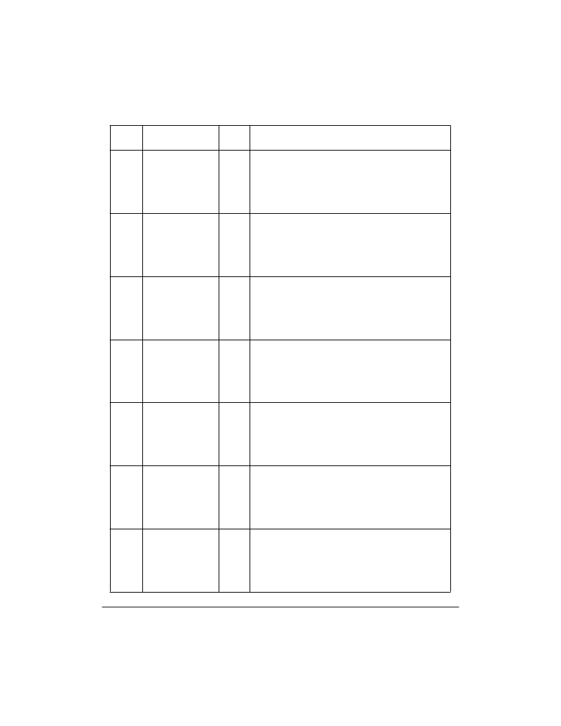
16
PCKEN
0
Memory interface parity checking/generation enable
0
Disables parity checking and parity generation for
transactions to DRAM/EDO/SDRAM memory. If ECC is
enabled, disables L2 parity checking.
1
Enables parity checking and generation for all memory
transactions to DRAM/EDO/SDRAM. If ECC is enabled,
enables L2 parity checking.
15–14
Bank 7 row
00
RAM bank 7 row address bit count. These bits indicate the
number of row address bits that are required by the RAM devices
in bank 7.
00 9 row bits
01 10 row bits
10 11 row bits
11 12 or 13 row bits
13–12
Bank 6 row
00
RAM bank 6 row address bit count. These bits indicate the
number of row address bits that are required by the RAM devices
in bank 6.
00 9 row bits
01 10 row bits
10 11 row bits
11 12 or 13 row bits
11–10
Bank 5 row
00
RAM bank 5 row address bit count. These bits indicate the
number of row address bits that are required by the RAM devices
in bank 5.
00 9 row bits
01 10 row bits
10 11 row bits
11 12 or 13 row bits
9–8
Bank 4 row
00
RAM bank 4 row address bit count. These bits indicate the
number of row address bits that are required by the RAM devices
in bank 4.
00 9 row bits
01 10 row bits
10 11 row bits
11 12 or 13 row bits
7–6
Bank 3 row
00
RAM bank 3 row address bit count. These bits indicate the
number of row address bits that are required by the RAM devices
in bank 3.
00 9 row bits
01 10 row bits
10 11 row bits
11 12 or 13 row bits
5–4
Bank 2 row
00
RAM bank 2 row address bit count. These bits indicate the
number of row address bits that are required by the RAM devices
in bank 2.
00 9 row bits
01 10 row bits
10 11 row bits
11 12 or 13 row bits
Table 3-31. Bit Settings for MCCR1—0xF0 (Continued)
Bit
Name
Reset
Value
Description
相關(guān)PDF資料 |
PDF描述 |
|---|---|
| MPC107 | 32-Bit Microprocessor(32位微處理器) |
| MPC505 | Highly Integrated, Low-Power, 32-Bit Microcontroller |
| MPC509 | Highly Integrated, Low-Power, 32-Bit Microcontroller |
| MPC5200BV400 | MPC5200 Hardware Specifications |
| MPC5200CBV266 | MPC5200 Hardware Specifications |
相關(guān)代理商/技術(shù)參數(shù) |
參數(shù)描述 |
|---|---|
| MPC106ARX66CE | 制造商:MOTOROLA 制造商全稱:Motorola, Inc 功能描述:PCI Bridge/Memory Controller |
| MPC106ARX66CG | 制造商:Freescale Semiconductor 功能描述: 制造商:Motorola Inc 功能描述: |
| MPC106ARX66DE | 制造商:MOTOROLA 制造商全稱:Motorola, Inc 功能描述:PCI Bridge/Memory Controller |
| MPC106ARX66DG | 制造商:MOTOROLA 制造商全稱:Motorola, Inc 功能描述:PCI Bridge/Memory Controller |
| MPC106ARX66TE | 制造商:MOTOROLA 制造商全稱:Motorola, Inc 功能描述:PCI Bridge/Memory Controller |
發(fā)布緊急采購,3分鐘左右您將得到回復(fù)。