- 您現(xiàn)在的位置:買賣IC網(wǎng) > PDF目錄296572 > ML6694CQ XC95108-10TQ100C - NOT RECOMMENDED for NEW DESIGN PDF資料下載
參數(shù)資料
| 型號: | ML6694CQ |
| 英文描述: | XC95108-10TQ100C - NOT RECOMMENDED for NEW DESIGN |
| 中文描述: | 100BASE - TX的物理層與5位接口 |
| 文件頁數(shù): | 8/12頁 |
| 文件大小: | 177K |
| 代理商: | ML6694CQ |
ML6694
5
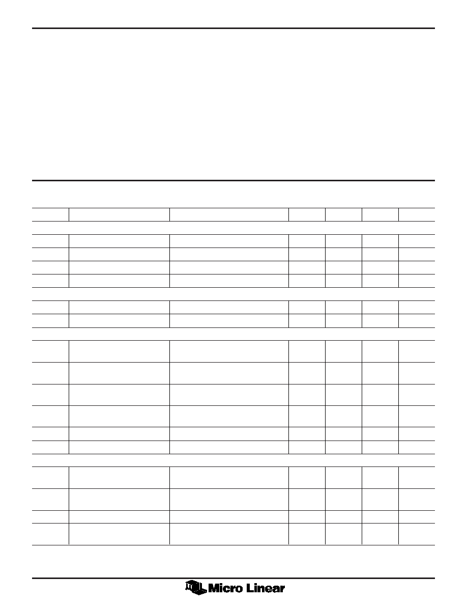
ABSOLUTE MAXIMUM RATINGS
Absolute maximum ratings are those values beyond which
the device could be permanently damaged. Absolute
maximum ratings are stress ratings only and functional
device operation is not implied.
VCC Supply Voltage Range .................... GND –0.3V to 6V
Input Voltage Range
Digital Inputs ....................... GND –0.3V to VCC + 0.3V
TPINP, TPINN, 10BTTXINN,
10BTTXINP ...................... GND –0.3V to VCC + 0.3V
Output Current
TPOUTP, TPOUTN .............................................. 60mA
All other outputs .................................................. 10mA
Junction Temperature .............................................. 150
°C
Storage Temperature ................................ –65
°C to 150°C
Lead Temperature (Soldering, 10 sec) ...................... 260
°C
OPERATING CONDITIONS
VCC Supply Voltage ............................................. 5V ± 5%
All VCC supply pins must be within 0.1V of each other.
All GND pins
must be within 0.1V of each other.
TA, Ambient temperature ................................ 0°C to 70°C
RGMSET ...................................................... 9.53k
± 1%
RTSET .......................................................... 2.49k
± 1%
Receive transformer insertion loss ........................ <–0.5dB
DC ELECTRICAL CHARACTERISTICS
Over full range of operating conditions unless otherwise specified (Note 1)
SYMBOL
PARAMETER
CONDITIONS
MIN
TYP
MAX
UNITS
TTL Inputs (TSM<4:0>, TXC, SEL10/
100, PWRDN, LPBK)
VIL
Input Low Voltage
IIL = –400A
0.8
V
VIH
Input High Voltage
IIH = 100A
2.0
V
IIL
Input Low Current
VIN = 0.4V
–200
A
IIH
Input High Current
VIN = 2.7V
100
A
TTL Outputs (RSM<4:0>, RXC, SDO)
VOL
Output Low Voltage
IOL = 4mA
0.4
V
VOH
Output High Voltage
IOH = –4mA
2.4
V
Receiver
VICM
TPINP/N Input Common-Mode
100
Termination across TPINP/N
VCC – 1.26
V
Voltage
VID
TPINP-TPINN Differential Input
–3.0
3.0
V
Voltage Range
RIDR
TPINP-TPINN Differential
10.0k
Input Resistance
IICM
TPINP/N Common-Mode Input
+10
A
Current
IRGM
RGMSET Input Current
RGMSET = 9.53k
130
A
IRT
RTSET Input Current
RTSET = 2.49k
500
A
Transmitter
ITD100
TPOUTP/N 100BASE-TX Mode
Note 2, 3
±19
±21
mA
Differential Output Current
ITD10
TPOUTP/N 10BASE-T
±55
±60
±65
mA
Mode Differential Output Current
ITOFF
TPOUTP/N Off-State Output
RL = 200, 1%
0
1.5
mA
ITXI
TPOUTP/N Differential Output
Current Imbalance
RL = 200, 1%
500
A
相關PDF資料 |
PDF描述 |
|---|---|
| ML6695CQ | 100BASE-X Fiber Physical Layer With 5-bit Interface |
| ML925J40F-11 | 1610 nm, LASER DIODE |
| MLF0805-082M | 1 ELEMENT, 0.082 uH, FERRITE-CORE, GENERAL PURPOSE INDUCTOR, SMD |
| MLF1206-R15K | 1 ELEMENT, 0.15 uH, FERRITE-CORE, GENERAL PURPOSE INDUCTOR, SMD |
| MLF1206-R18K | 1 ELEMENT, 0.18 uH, FERRITE-CORE, GENERAL PURPOSE INDUCTOR, SMD |
相關代理商/技術參數(shù) |
參數(shù)描述 |
|---|---|
| ML6695 | 制造商:MICRO-LINEAR 制造商全稱:MICRO-LINEAR 功能描述:100BASE-X Fiber Physical Layer With 5-bit Interface |
| ML6695CQ | 制造商:MICRO-LINEAR 制造商全稱:MICRO-LINEAR 功能描述:100BASE-X Fiber Physical Layer With 5-bit Interface |
| ML6696 | 制造商:MICRO-LINEAR 制造商全稱:MICRO-LINEAR 功能描述:100BASE-X Fiber Physical Layer |
| ML6696CH | 制造商:MICRO-LINEAR 制造商全稱:MICRO-LINEAR 功能描述:100BASE-X Fiber Physical Layer |
| ML6696CQ | 制造商:Micro Linear 功能描述:DATACOM, INTERFACE CIRCUIT, PQCC52 |
發(fā)布緊急采購,3分鐘左右您將得到回復。