- 您現(xiàn)在的位置:買賣IC網(wǎng) > PDF目錄65810 > MK1581-01GITR 2.048 MHz, OTHER CLOCK GENERATOR, PDSO16 PDF資料下載
參數(shù)資料
| 型號: | MK1581-01GITR |
| 元件分類: | 時(shí)鐘產(chǎn)生/分配 |
| 英文描述: | 2.048 MHz, OTHER CLOCK GENERATOR, PDSO16 |
| 封裝: | 4.40 MM, 0.65 MM PITCH, MO-153, TSSOP-16 |
| 文件頁數(shù): | 6/10頁 |
| 文件大小: | 152K |
| 代理商: | MK1581-01GITR |
Low Phase Noise T1 / E1 Clock Generator
MDS 1581-01 C
5
Revision 050803
Integrated Circuit Systems, Inc. ● 525 Race Street, San Jose, CA 95126 ● tel (408) 295-9800 ●
www.icst.com
MK1581-01
A “normalized” PLL loop bandwidth may be calculated
as follows:
The “normalized” bandwidth (NBW) equation above
does not take into account the effects of damping factor
or the second pole. NBW is approximately equal to the
actual -3dB bandwidth of the loop when the damping
factor is about 5 and C2 is very small. In most
applications, NBW is about 75% of the actual -3dB
bandwidth. However, NBW does provide a useful
approximation of filter performance.
The loop damping factor is calculated as follows:
Where:
RS = Value of resistor in loop filter (Ohms)
ICP = Charge pump current (amps)
(refer to Charge Pump Current Table, below)
N = Crystal multiplier shown in the above table
CS = Value of capacitor CS in loop filter
(Farads)
As a general rule, the following relationship should be
maintained between components CS and CP in the loop
filter:
Charge Pump Current Table
Special considerations must be made in choosing loop
components CS and CP.
These recommendations can be found in the design
aid tools section of www.icst.com.
Series Termination Resistor
Clock output traces over one inch should use series
termination. To series terminate a 50
W trace (a
commonly used trace impedance), place a 33
W resistor
in series with the clock line, as close to the clock output
pin as possible. The nominal impedance of the clock
output is 20
W. (The optional series termination resistor
is not shown in the External Component Schematic.)
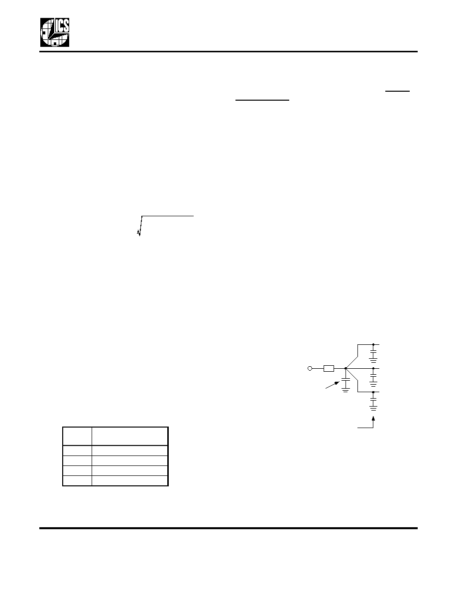
Decoupling Capacitors
As with any high performance mixed-signal IC, the
MK1581-01 must be isolated from system power
supply noise to perform optimally.
Decoupling capacitors of 0.01F must be connected
between each VDD and the PCB ground plane. To
further guard against interfering system supply noise,
the MK1581-01 should use one common connection to
the PCB power plane as shown in the diagram on the
next page. The ferrite bead and bulk capacitor help
reduce lower frequency noise in the supply that can
lead to output clock phase modulation.
Recommended Power Supply Connection
for Optimal Device Performance
Crystal Load Capacitors
The device crystal connections should include pads for
small capacitors from X1 to ground and from X2 to
ground, shown as CL in the External Component
Schematic. These capacitors are used to adjust the
stray capacitance of the board to match the nominally
RSET
Charge Pump Current
(ICP)
1.4 M
W
10
mA
680 k
W
20
mA
540 k
W
25
mA
120 k
W
100
mA
NBW
RS ICP
575
N
---------------------------------------
=
Damping Factor
RS
625
I
CP
CS
N
-----------------------------------------
=
CP
CS
20
------
=
C onnection to 3.3V
Pow er Plane
Ferrite
Bead
B ulk D ecoupling C apac itor
(such as 1
F Tantalum)
V DD P in
0.01
F Decoupling Capacitors
相關(guān)PDF資料 |
PDF描述 |
|---|---|
| MK1581-01GI | 2.048 MHz, OTHER CLOCK GENERATOR, PDSO16 |
| MK1704A | 140 MHz, OTHER CLOCK GENERATOR, PDSO8 |
| MK1705A | 167 MHz, VIDEO CLOCK GENERATOR, PDSO8 |
| MK1705ALFTR | 167 MHz, VIDEO CLOCK GENERATOR, PDSO8 |
| MK1705ATR | 167 MHz, VIDEO CLOCK GENERATOR, PDSO8 |
相關(guān)代理商/技術(shù)參數(shù) |
參數(shù)描述 |
|---|---|
| MK159 | 制造商:Velleman Inc 功能描述:Brain Game Kit |
| MK15-B-0 | 制造商:MEDER 制造商全稱:Meder Electronic 功能描述:MK Reed Sensors |
| MK15-B-0_DE | 制造商:MEDER 制造商全稱:Meder Electronic 功能描述:(deutsch) MK Reed Sensor |
| MK15-B-1 | 功能描述:近程傳感器 1 Form A Flat Leads Slot Mount AT 1015 RoHS:否 制造商:Vishay Semiconductors 感應(yīng)方式:Optical 感應(yīng)距離:1 mm to 200 mm 電源電壓:2.5 V to 3.6 V 安裝風(fēng)格:SMD/SMT 輸出配置:Digital 最大工作溫度:+ 85 C 最小工作溫度:- 25 C 系列:VCNL3020 |
| MK15-B-1_10 | 制造商:MEDER 制造商全稱:Meder Electronic 功能描述:Reed Sensors for SMD Mounting |
發(fā)布緊急采購,3分鐘左右您將得到回復(fù)。