- 您現(xiàn)在的位置:買賣IC網(wǎng) > PDF目錄359155 > MCZ33291LEG (飛思卡爾半導(dǎo)體(中國)有限公司) Eight-Output Switch with Serial Peripheral Interface I/O PDF資料下載
參數(shù)資料
| 型號: | MCZ33291LEG |
| 廠商: | 飛思卡爾半導(dǎo)體(中國)有限公司 |
| 英文描述: | Eight-Output Switch with Serial Peripheral Interface I/O |
| 中文描述: | 8輸出開關(guān)串行外設(shè)接口的I / O |
| 文件頁數(shù): | 13/25頁 |
| 文件大小: | 389K |
| 代理商: | MCZ33291LEG |
Analog Integrated Circuit Device Data
Freescale Semiconductor
13
33291L
FUNCTIONAL DESCRIPTION
FUNCTIONAL PIN DESCRIPTION
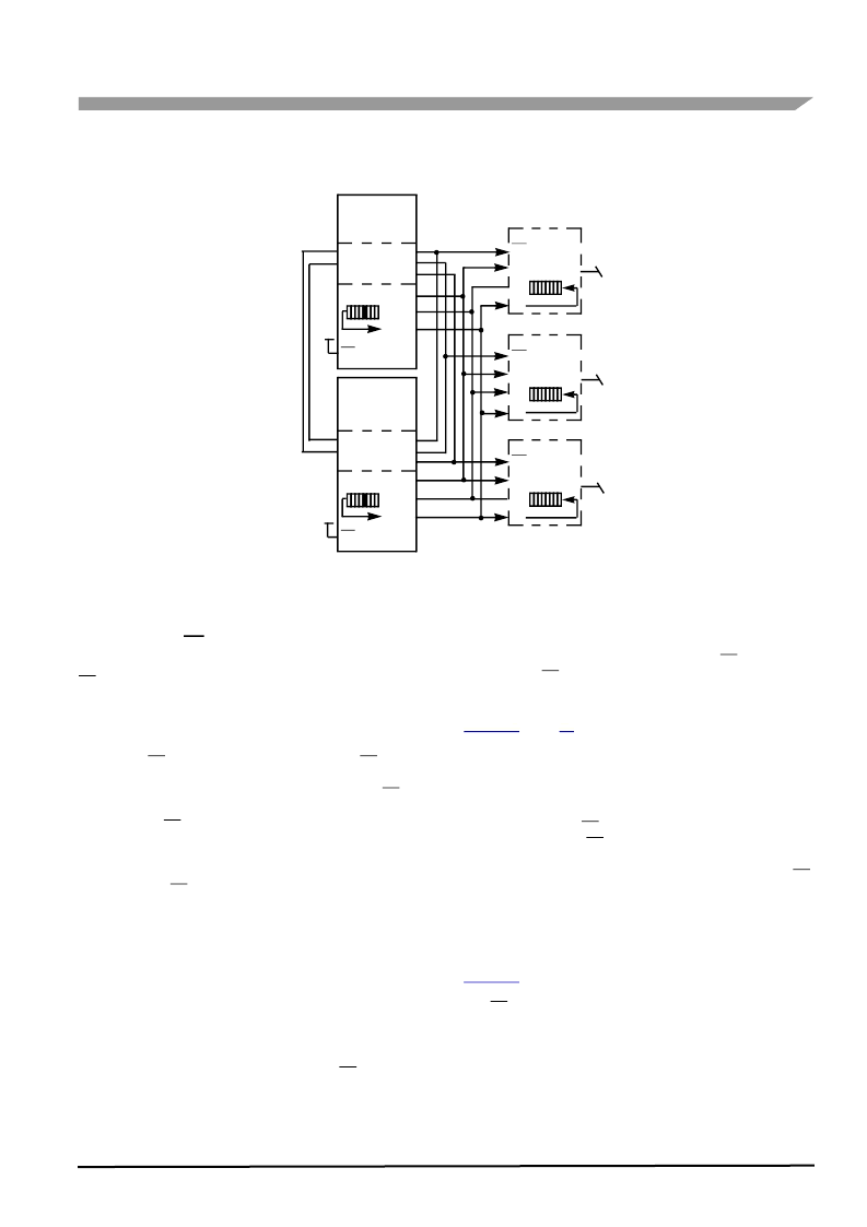
Figure 15. Multiple MCU SPI Control
FUNCTIONAL PIN DESCRIPTION
CHIP SELECT (CS)
The 33291L receives its MCU communication through the
CS
pin. Whenever this pin is in a logic low state, data can be
transferred from the MCU to the 33291L by way of the SI pin
and from the 33291L to the MCU through the SO pin.
Clocked-in data from the MCU is transferred from the 33291L
Shift register and latched into the power outputs on the rising
edge of the
CS
signal. On the falling edge of the
CS
signal,
drain status information is transferred from the power outputs
then loaded into the Shift register of the device. The
CS
pin
also controls the output driver of the serial output (SO) pin.
Whenever the
CS
pin goes to a logic low state, the SO pin
output driver is enabled allowing information to be transferred
from the 33291L to the MCU. To avoid data corruption or the
generation of spurious data, it is essential the high-to-low
transition of the
CS
signal occur only when SCLK is in a logic
low state.
SYSTEM CLOCK (SCLK)
The system clock (SCLK) pin clocks the internal shift
registers of the 33291L. The serial input (SI) pin accepts data
into the Input Shift register on the falling edge of the SCLK
signal while the serial output (SO) pin shifts data information
out of the SO line driver on the rising edge of the SCLK signal.
False clocking of the Shift register must be avoided to
guarantee validity of data. It is essential the SCLK pin be in a
logic low state whenever the chip select bar (
CS
) pin makes
any transition. For this reason, it is recommended, though not
absolutely necessary, the SCLK pin be kept in a low logic
state as long as the device is not accessed (
CS
in logic high
state). When
CS
is in a logic high state, signals at the SCLK
and SI pins are ignored and SO is tri-stated (high
impedance). See the Data Transfer Timing diagram in
Figure 17
, page
16
.
SERIAL INSTRUCTION (SI)
This pin is for the input of serial instruction (SI) data. SI is
read on the falling edge of SCLK. A logic high state present
on this pin when the SCLK signal rises will program a specific
output OFF. In turn,
CS
pin turns OFF the specific output on
the rising edge of the
CS
signal. Conversely, a logic low state
present on the SI pin will program the output ON, In turn, the
pin turns ON the specific output on the rising edge of the
CS
signal.
To program the eight outputs of the 33291L ON or OFF, an
8-bit serial stream of data is required to be synchronously
entered into the SI pin starting with Output 7, followed by
Output 6, Output 5, and so on, to Output 0. Referring to
Figure 17
, the DO bit is the most significant bit (MSB)
corresponding to Output 7. For each rise of the SCLK signal,
with
CS
held in a logic low state, a data-bit instruction (ON or
OFF) is synchronously loaded into the Shift register per the
data-bit SI state. The Shift register is full after eight bits of
information have been entered. To preserve data integrity,
care should be taken to not transition SI as SCLK transitions
from a low-to-high logic state.
SI
SO
SCLK
CS
8-Bit
33291
SI
SO
SCLK
CS
8-Bit
33291
SI
SO
SCLK
CS
8-Bit
33291
8 Outputs
8 Outputs
8 Outputs
V
DD
V
DD
B0
B1
B0
B1
MC68XX
Microcontroller
SPI
(Master)
A0
A1
A2
A0
A1
A2
MC68XX
Microcontroller
SPI
(Alternate Master)
Ports
8-Bit
Ports
SCLK
MISO
MOSI
SCLK
MISO
MOSI
SS
SS
8-Bit
相關(guān)PDF資料 |
PDF描述 |
|---|---|
| MCZ33390EF | Class B Serial Transceiver |
| MCZ33395EW | Three-Phase Gate Driver IC |
| MCZ33399EF | Local Interconnect Network (LIN) Physical Interface |
| MCZ33661EF | Local Area Network (LIN) Enhanced Physical Interface with Selectable Slew Rate |
| MCZ33689DEW | System Basis Chip with LIN Transceiver |
相關(guān)代理商/技術(shù)參數(shù) |
參數(shù)描述 |
|---|---|
| MCZ33291LEGR2 | 功能描述:電源開關(guān) IC - 配電 BASIC OCTAL SER SW RoHS:否 制造商:Exar 輸出端數(shù)量:1 開啟電阻(最大值):85 mOhms 開啟時間(最大值):400 us 關(guān)閉時間(最大值):20 us 工作電源電壓:3.2 V to 6.5 V 電源電流(最大值): 最大工作溫度:+ 85 C 安裝風(fēng)格:SMD/SMT 封裝 / 箱體:SOT-23-5 |
| MCZ33298EG | 功能描述:電源開關(guān) IC - 配電 OCTAL SERIAL SWITCH RoHS:否 制造商:Exar 輸出端數(shù)量:1 開啟電阻(最大值):85 mOhms 開啟時間(最大值):400 us 關(guān)閉時間(最大值):20 us 工作電源電壓:3.2 V to 6.5 V 電源電流(最大值): 最大工作溫度:+ 85 C 安裝風(fēng)格:SMD/SMT 封裝 / 箱體:SOT-23-5 |
| MCZ33298EG/R2 | 制造商:FREESCALE 制造商全稱:Freescale Semiconductor, Inc 功能描述:Eight Output Switch with Serial Peripheral Interface I/O |
| MCZ33298EGR2 | 功能描述:電源開關(guān) IC - 配電 OCTAL SERIAL SWITCH RoHS:否 制造商:Exar 輸出端數(shù)量:1 開啟電阻(最大值):85 mOhms 開啟時間(最大值):400 us 關(guān)閉時間(最大值):20 us 工作電源電壓:3.2 V to 6.5 V 電源電流(最大值): 最大工作溫度:+ 85 C 安裝風(fēng)格:SMD/SMT 封裝 / 箱體:SOT-23-5 |
| MCZ3334EF | 功能描述:基準(zhǔn)電壓& 基準(zhǔn)電流 HI ENERGY IGNITION RoHS:否 制造商:STMicroelectronics 產(chǎn)品:Voltage References 拓?fù)浣Y(jié)構(gòu):Shunt References 參考類型:Programmable 輸出電壓:1.24 V to 18 V 初始準(zhǔn)確度:0.25 % 平均溫度系數(shù)(典型值):100 PPM / C 串聯(lián) VREF - 輸入電壓(最大值): 串聯(lián) VREF - 輸入電壓(最小值): 分流電流(最大值):60 mA 最大工作溫度:+ 125 C 封裝 / 箱體:SOT-23-3L 封裝:Reel |
發(fā)布緊急采購,3分鐘左右您將得到回復(fù)。