- 您現(xiàn)在的位置:買賣IC網(wǎng) > PDF目錄354436 > MCM69C232TQ20 (MOTOROLA INC) 4K x 64 CAM PDF資料下載
參數(shù)資料
| 型號(hào): | MCM69C232TQ20 |
| 廠商: | MOTOROLA INC |
| 元件分類: | DRAM |
| 英文描述: | 4K x 64 CAM |
| 中文描述: | 4K X 64 CONTENT ADDRESSABLE SRAM, 160 ns, PQFP100 |
| 封裝: | TQFP-100 |
| 文件頁(yè)數(shù): | 12/16頁(yè) |
| 文件大小: | 175K |
| 代理商: | MCM69C232TQ20 |
第1頁(yè)第2頁(yè)第3頁(yè)第4頁(yè)第5頁(yè)第6頁(yè)第7頁(yè)第8頁(yè)第9頁(yè)第10頁(yè)第11頁(yè)當(dāng)前第12頁(yè)第13頁(yè)第14頁(yè)第15頁(yè)第16頁(yè)
MCM69F817
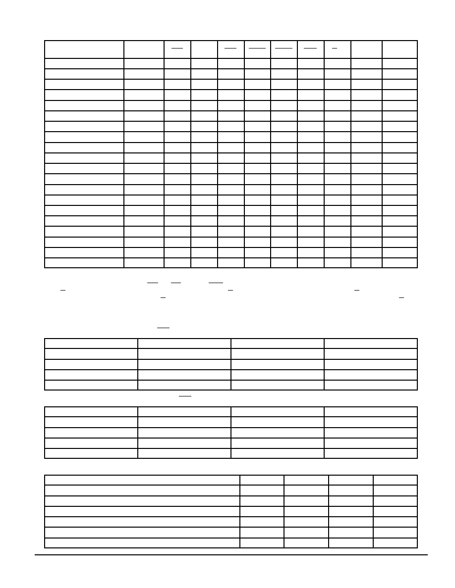
5
MOTOROLA FAST SRAM
TRUTH TABLE (See Notes 1 Through 5)
Next Cycle
Address
Used
SE1
SE2
SE3
ADSP
ADSC
ADV
G 3
DQx
Write 2, 4
Deselect
None
1
X
0
X
High–Z
X
Deselect
None
0
X
1
0
X
High–Z
X
Deselect
None
0
X
0
X
High–Z
X
Deselect
None
X
1
0
X
High–Z
X
Deselect
None
X
0
X
1
0
X
High–Z
X
Begin Read
External
0
1
0
X
High–Z
X5
Begin Read
External
0
1
0
1
0
X
High–Z
READ5
Continue Read
Next
X
1
0
1
High–Z
READ
Continue Read
Next
X
1
0
DQ
READ
Continue Read
Next
1
X
1
0
1
High–Z
READ
Continue Read
Next
1
X
1
0
DQ
READ
Suspend Read
Current
X
1
High–Z
READ
Suspend Read
Current
X
1
0
DQ
READ
Suspend Read
Current
1
X
1
High–Z
READ
Suspend Read
Current
1
X
1
0
DQ
READ
Begin Write
External
0
1
0
1
0
X
High–Z
WRITE
Continue Write
Next
X
1
0
X
High–Z
WRITE
Continue Write
Next
1
X
1
0
X
High–Z
WRITE
Suspend Write
Current
X
1
X
High–Z
WRITE
Suspend Write
Current
1
X
1
X
High–Z
WRITE
NOTES:
1. X = don’t care. 1 = logic high. 0 = logic low.
2. Write is defined as either (a) any SBx and SW low or (b) SGW is low.
3. G is an asynchronous signal and is not sampled by the clock K. G drives the bus immediately (tGLQX) following G going low.
4. On write cycles that follow read cycles, G must be negated prior to the start of the write cycle to ensure proper write data setup times. G must
also remain negated at the completion of the write cycle to ensure proper write data hold times.
5. This read assumes the RAM was previously deselected.
LINEAR BURST ADDRESS TABLE (LBO = VSS)
1st Address (External)
2nd Address (Internal)
3rd Address (Internal)
4th Address (Internal)
X . . . X00
X . . . X01
X . . . X10
X . . . X11
X . . . X01
X . . . X10
X . . . X11
X . . . X00
X . . . X10
X . . . X11
X . . . X00
X . . . X01
X . . . X11
X . . . X00
X . . . X01
X . . . X10
INTERLEAVED BURST ADDRESS TABLE (LBO = VDD)
1st Address (External)
2nd Address (Internal)
3rd Address (Internal)
4th Address (Internal)
X . . . X00
X . . . X01
X . . . X10
X . . . X11
X . . . X01
X . . . X00
X . . . X11
X . . . X10
X . . . X11
X . . . X00
X . . . X01
X . . . X11
X . . . X10
X . . . X01
X . . . X00
WRITE TRUTH TABLE
Cycle Type
SGW
SW
SBa
SBb
Read
H
X
Read
H
L
H
Write Byte a
H
L
H
Write Byte b
H
L
H
L
Write All Bytes
H
L
Write All Bytes
L
X
相關(guān)PDF資料 |
PDF描述 |
|---|---|
| MCM69C232TQ20R | 4K x 64 CAM |
| MCM69C432 | 16K x 64 CAM |
| MCM69C432TQ20 | 16K x 64 CAM |
| MCM69C432TQ20R | 16K x 64 CAM |
| MCM69D536 | 32K x 36 Bit Synchronous Dual I/O, Dual Address SRAM |
相關(guān)代理商/技術(shù)參數(shù) |
參數(shù)描述 |
|---|---|
| MCM69C232TQ20R | 制造商:MOTOROLA 制造商全稱:Motorola, Inc 功能描述:4K x 64 CAM |
| MCM69C233TQ15 | 制造商:Rochester Electronics LLC 功能描述:- Bulk |
| MCM69C233WD | 制造商:MOTOROLA 制造商全稱:Motorola, Inc 功能描述:MPC8260 PowerQUICC II-TM to CAM Interfacing ? MCM69C233 |
| MCM69C233WP | 制造商:MOTOROLA 制造商全稱:Motorola, Inc 功能描述:MPC8260 PowerQUICC II-TM to CAM Interfacing ? MCM69C233 |
| MCM69C432 | 制造商:MOTOROLA 制造商全稱:Motorola, Inc 功能描述:16K x 64 CAM |
發(fā)布緊急采購(gòu),3分鐘左右您將得到回復(fù)。