- 您現(xiàn)在的位置:買賣IC網(wǎng) > PDF目錄45193 > MB91F366GBPMT 32-BIT, FLASH, 64 MHz, RISC MICROCONTROLLER, PQFP120 PDF資料下載
參數(shù)資料
| 型號(hào): | MB91F366GBPMT |
| 元件分類: | 微控制器/微處理器 |
| 英文描述: | 32-BIT, FLASH, 64 MHz, RISC MICROCONTROLLER, PQFP120 |
| 封裝: | PLASTIC, LQFP-120 |
| 文件頁(yè)數(shù): | 127/239頁(yè) |
| 文件大小: | 3093K |
| 代理商: | MB91F366GBPMT |
第1頁(yè)第2頁(yè)第3頁(yè)第4頁(yè)第5頁(yè)第6頁(yè)第7頁(yè)第8頁(yè)第9頁(yè)第10頁(yè)第11頁(yè)第12頁(yè)第13頁(yè)第14頁(yè)第15頁(yè)第16頁(yè)第17頁(yè)第18頁(yè)第19頁(yè)第20頁(yè)第21頁(yè)第22頁(yè)第23頁(yè)第24頁(yè)第25頁(yè)第26頁(yè)第27頁(yè)第28頁(yè)第29頁(yè)第30頁(yè)第31頁(yè)第32頁(yè)第33頁(yè)第34頁(yè)第35頁(yè)第36頁(yè)第37頁(yè)第38頁(yè)第39頁(yè)第40頁(yè)第41頁(yè)第42頁(yè)第43頁(yè)第44頁(yè)第45頁(yè)第46頁(yè)第47頁(yè)第48頁(yè)第49頁(yè)第50頁(yè)第51頁(yè)第52頁(yè)第53頁(yè)第54頁(yè)第55頁(yè)第56頁(yè)第57頁(yè)第58頁(yè)第59頁(yè)第60頁(yè)第61頁(yè)第62頁(yè)第63頁(yè)第64頁(yè)第65頁(yè)第66頁(yè)第67頁(yè)第68頁(yè)第69頁(yè)第70頁(yè)第71頁(yè)第72頁(yè)第73頁(yè)第74頁(yè)第75頁(yè)第76頁(yè)第77頁(yè)第78頁(yè)第79頁(yè)第80頁(yè)第81頁(yè)第82頁(yè)第83頁(yè)第84頁(yè)第85頁(yè)第86頁(yè)第87頁(yè)第88頁(yè)第89頁(yè)第90頁(yè)第91頁(yè)第92頁(yè)第93頁(yè)第94頁(yè)第95頁(yè)第96頁(yè)第97頁(yè)第98頁(yè)第99頁(yè)第100頁(yè)第101頁(yè)第102頁(yè)第103頁(yè)第104頁(yè)第105頁(yè)第106頁(yè)第107頁(yè)第108頁(yè)第109頁(yè)第110頁(yè)第111頁(yè)第112頁(yè)第113頁(yè)第114頁(yè)第115頁(yè)第116頁(yè)第117頁(yè)第118頁(yè)第119頁(yè)第120頁(yè)第121頁(yè)第122頁(yè)第123頁(yè)第124頁(yè)第125頁(yè)第126頁(yè)當(dāng)前第127頁(yè)第128頁(yè)第129頁(yè)第130頁(yè)第131頁(yè)第132頁(yè)第133頁(yè)第134頁(yè)第135頁(yè)第136頁(yè)第137頁(yè)第138頁(yè)第139頁(yè)第140頁(yè)第141頁(yè)第142頁(yè)第143頁(yè)第144頁(yè)第145頁(yè)第146頁(yè)第147頁(yè)第148頁(yè)第149頁(yè)第150頁(yè)第151頁(yè)第152頁(yè)第153頁(yè)第154頁(yè)第155頁(yè)第156頁(yè)第157頁(yè)第158頁(yè)第159頁(yè)第160頁(yè)第161頁(yè)第162頁(yè)第163頁(yè)第164頁(yè)第165頁(yè)第166頁(yè)第167頁(yè)第168頁(yè)第169頁(yè)第170頁(yè)第171頁(yè)第172頁(yè)第173頁(yè)第174頁(yè)第175頁(yè)第176頁(yè)第177頁(yè)第178頁(yè)第179頁(yè)第180頁(yè)第181頁(yè)第182頁(yè)第183頁(yè)第184頁(yè)第185頁(yè)第186頁(yè)第187頁(yè)第188頁(yè)第189頁(yè)第190頁(yè)第191頁(yè)第192頁(yè)第193頁(yè)第194頁(yè)第195頁(yè)第196頁(yè)第197頁(yè)第198頁(yè)第199頁(yè)第200頁(yè)第201頁(yè)第202頁(yè)第203頁(yè)第204頁(yè)第205頁(yè)第206頁(yè)第207頁(yè)第208頁(yè)第209頁(yè)第210頁(yè)第211頁(yè)第212頁(yè)第213頁(yè)第214頁(yè)第215頁(yè)第216頁(yè)第217頁(yè)第218頁(yè)第219頁(yè)第220頁(yè)第221頁(yè)第222頁(yè)第223頁(yè)第224頁(yè)第225頁(yè)第226頁(yè)第227頁(yè)第228頁(yè)第229頁(yè)第230頁(yè)第231頁(yè)第232頁(yè)第233頁(yè)第234頁(yè)第235頁(yè)第236頁(yè)第237頁(yè)第238頁(yè)第239頁(yè)
MB91360G Series
212
■ ELECTRICAL CHARACTERISTICS
1.
Absolute Maximum Ratings
*1 : Making full use of the allowed static DC correct into digital I/O will lead to lower values for VIDIG Min.
*2 :
Applicable to pins : D0 to D31, A0 to A20, CS0X to CS6X, RDY, BGRNTX, BRQ, RDX, WR0X to WR3X, AS,
ALE, CLK, DREQ0, DACK0, DEOP0, INT0 to INT7, SGO, SGA, SDA, SCL, SOT0, SIN0,
SCK0, OCPA0 to OCPA3, TX0, TX1, RX0, RX1, SOT3, SOT4, SIN3, SIN4,
SCK3, SCK4, LED0 to LED7 (MB91F362GB only) , IN0 to IN3 (MB91F362GB only) ,
OUT0 to OUT3 (MB91F362GB only) , OCPA4 to OCPA7 (MB91F362GB only) ,
SOT1, SOT2 (MB91F362GB only) , SIH1, SIH2 (MB91F362GB only) ,
SCK1, SCK2 (MB91F362GB only) , PWM1P0 to PWM1P3 (MB91F362GB only) ,
PWM1M0 to PWM1M3 (MB91F362GB only) , PWM2P0 to PWM2P3 (MB91F362GB only) ,
PWM2M0 to PWM2M3 (MB91F362GB only)
Use within recommended operating conditions.
Use at DC voltage (current) .
The +B signal should always be applied with a limiting resistance placed between the +B signal and the
microcontroller.
The value of the limiting resistance should be set so that when the +B signal is applied the input current to
the microcontroller pin does not exceed rated values, either instantaneously or for prolonged periods.
Note that when the microcontroller drive current is low, such as in the power saving modes, the +B input
potential may pass through the protective diode and increase the potential at the VCC pin, and this may affect
other devices.
Note that if a +B signal is input when the microcontroller current is off (not fixed at 0 V) , the power supply is
provided from the pins, so that incomplete operation may result.
Note that if the +B input is applied during power-on, the power supply is provided from the pins and the resulting
supply voltage may not be sufficient to operate the power-on reset.
Care must be taken not to leave the +B input pin open.
Note that analog system input/output pins other than the A/D input pins (LCD drive pins, comparator input
pins, etc.) cannot accept +B signal input.
(Continued)
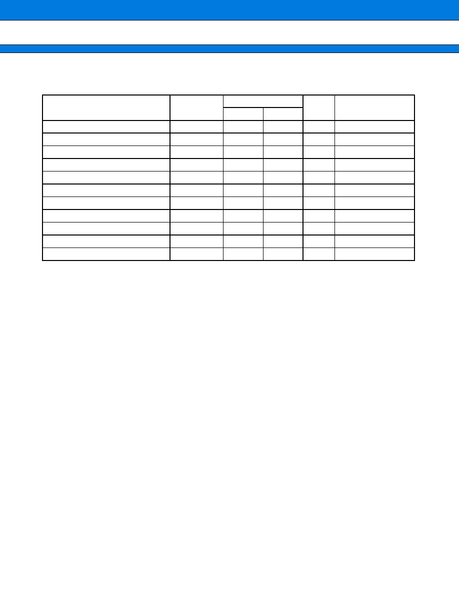
Parameter
Symbol
Rating
Unit
Condition
Min
Max
Digital supply voltage
VDD-VSS
0.3
+6.0
V
External interface supply
VDD35-VSS
0.3
+6.0
V
*4
Stepper motor control supply voltage
HVDD-HVSS
0.3
+6.5
V
Storage temperature
Tstg
55
+125
°C
Power consumption
PTOT
*3
W
TA
= +25°C
Digital input voltage
VIDIG
0.3*1
+5.8
V
VSS
= 0 V, VDD = 5 V
Analog input voltage
VIA
0.3
+5.8
V
AVSS
= 0 V, AVCC = 5 V
Analog supply voltage
AVCC-AVSS
0.3
+5.8
V
AVSS
= 0 V
Analog reference voltage
VREFH/L-VSSA
0.3
+5.8
V
AVSS
= 0 V
Static DC current into digital I/O
II/ODC
2.0
+2.0
mA
ΣII/ODC < ISRUN, *2
Static total DC current into digital I/O
ΣII/ODC
20
mA
*2
相關(guān)PDF資料 |
PDF描述 |
|---|---|
| MB91F364GPMT | 32-BIT, FLASH, 64 MHz, RISC MICROCONTROLLER, PQFP120 |
| MB91F365GBPMT | 32-BIT, FLASH, 64 MHz, RISC MICROCONTROLLER, PQFP120 |
| MB91F467DBPVSR-GSE2 | 32-BIT, FLASH, 100 MHz, RISC MICROCONTROLLER, PQFP208 |
| MB91F467DAPVSR-GSE2 | 32-BIT, FLASH, 100 MHz, RISC MICROCONTROLLER, PQFP208 |
| MB91F467PAPMC-GSE2 | RISC MICROCONTROLLER, PQFP176 |
相關(guān)代理商/技術(shù)參數(shù) |
參數(shù)描述 |
|---|---|
| MB91F366GBPMT-ES | 制造商:FUJITSU 功能描述: |
| MB91F367GA | 制造商:FUJITSU 制造商全稱:Fujitsu Component Limited. 功能描述:32-BIT MICROCONTROLLER |
| MB91F367GB | 制造商:FUJITSU 制造商全稱:Fujitsu Component Limited. 功能描述:32-bit RISC Microcontroller |
| MB91F367GBPMT | 制造商:FUJITSU 制造商全稱:Fujitsu Component Limited. 功能描述:32-bit RISC Microcontroller |
| MB91F368GA | 制造商:FUJITSU 制造商全稱:Fujitsu Component Limited. 功能描述:32-BIT MICROCONTROLLER |
發(fā)布緊急采購(gòu),3分鐘左右您將得到回復(fù)。