- 您現(xiàn)在的位置:買賣IC網(wǎng) > PDF目錄384702 > MAX79C (Maxim Integrated Products, Inc.) 3.0V/3.3V Adjustable Microprocessor Supervisory Circuits PDF資料下載
參數(shù)資料
| 型號: | MAX79C |
| 廠商: | Maxim Integrated Products, Inc. |
| 英文描述: | 3.0V/3.3V Adjustable Microprocessor Supervisory Circuits |
| 中文描述: | 3.0V/3.3V可調(diào)微處理器監(jiān)控電路 |
| 文件頁數(shù): | 11/20頁 |
| 文件大小: | 150K |
| 代理商: | MAX79C |
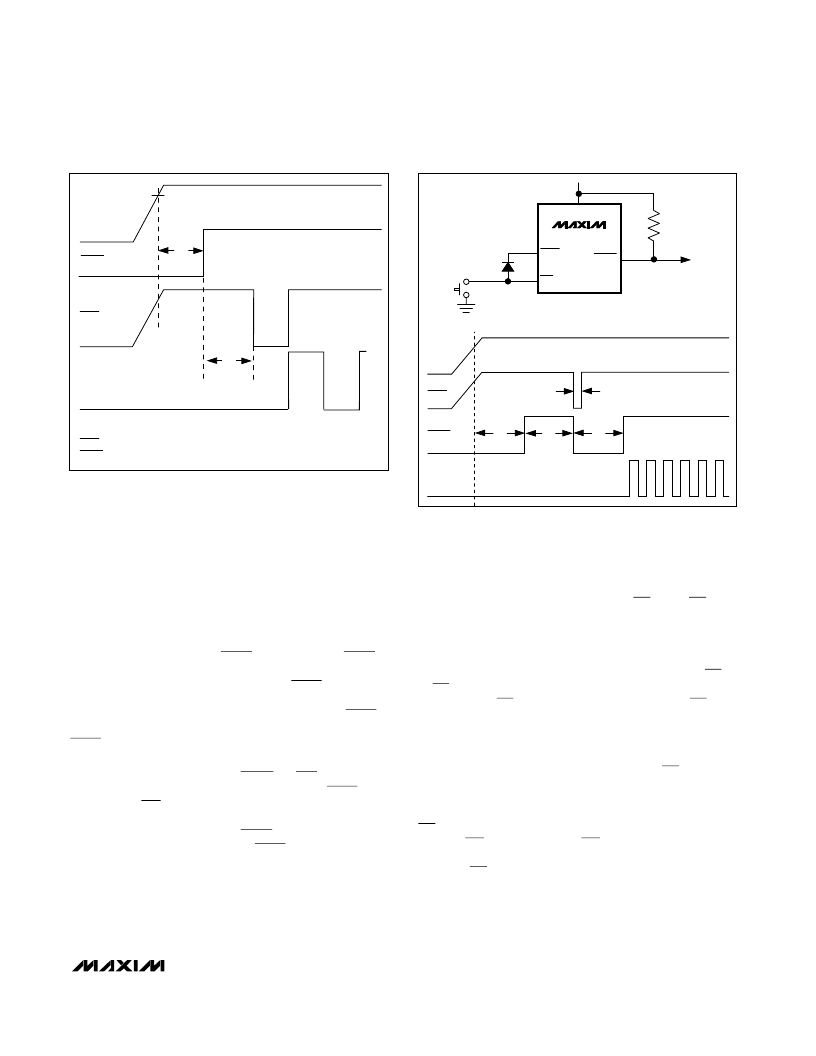
either when a reset occurs or when a transition (low-to-
high or high-to-low) takes place at WDI. As long as
reset is asserted, the timer remains cleared and does
not count. As soon as reset is released or WDI
changes state, the timer starts counting (Figure 5).
WDI can detect pulses as short as 100ns. Unlike the
5V MAX690 family, the watchdog function
cannot
be
disabled.
Watc hdog Output (MAX 793/MAX 794)
In the MAX793/MAX794, WDO remains high (WDO is
pulled up to V
CC
) if there is a transition or pulse at WDI
during the watchdog timeout period. WDO goes low if
no transition occurs at WDI during the watchdog timeout
period. The watchdog function is disabled and WDO is
a logic high when reset is asserted if V
CC
is above V
SW
.
WDO is a logic low when V
CC
is below V
SW
.
If a system reset is desired on every watchdog fault,
simply diode-OR connect WDO to MR (Figure 6).
When a watchdog fault occurs in this mode, WDO goes
low, pulling MR low, which causes a reset pulse to be
issued. Ten microseconds after reset is asserted, the
watchdog timer clears and WDO returns high. This
delay results in a 10μs pulse at WDO, allowing external
circuitry to “capture” a watchdog fault indication. A
continuous high or low on WDI will cause 200ms reset
pulses to be issued every 1.6sec.
Chip-Enable S ignal Gating
Internal gating of chip-enable (CE) signals prevents erro-
neous data from corrupting CMOS RAM in the event of an
undervoltage condition. The MAX793/MAX794/MAX795
use a series transmission gate from CE IN to CE OUT
(Figure 7). During normal operation (reset not asserted),
the CE transmission gate is enabled and passes all CE
transitions. When reset is asserted, this path becomes
disabled, preventing erroneous data from corrupting the
CMOS RAM. The short CE propagation delay from CE IN
to CE OUT enables these μP supervisors to be used with
most μPs. If CE IN is low when reset asserts, CE OUT
remains low for typically 10μs to permit completion of the
current write cycle.
Chip-Enable Input
The CE transmission gate is disabled and CE IN is high
impedance (disabled mode) while reset is asserted.
During a power-down sequence when V
CC
passes the
reset threshold, the CE transmission gate disables and
CE IN immediately becomes high impedance if the volt-
age at CE IN is high. If CE IN is low when reset
asserts, the CE transmission gate will disable at the
moment CE IN goes high, or 10μs after reset asserts,
whichever occurs first (Figure 8). This permits the cur-
rent write cycle to complete during power-down.
M
3.0V /3.3V Adjustable Mic roproc essor
S upervisory Circ uits
______________________________________________________________________________________
11
V
CC
V
RST
RESET
t
WD
WDO
WDI
WDOCONNECTED TO
μ
P INTERRUPT
RESET PULLED UP TOV
CC
t
RP
Figure 5. Watchdog Timing Relationship
V
CC
V
CC
RESET
WDO
WDO
4.7k
TO
μ
P
MR
RESET
WDI
t
RP
t
RP
t
WP
~
10
μ
s
MAX793/MAX794
Figure 6. Generating a Reset on Each Watchdog Fault
相關(guān)PDF資料 |
PDF描述 |
|---|---|
| MAX79E | 3.0V/3.3V Adjustable Microprocessor Supervisory Circuits |
| MAX794ESE | 3.0V/3.3V Adjustable Microprocessor Supervisory Circuits |
| MAX794CPE | Quadruple 2-Input Exclusive-OR Gates 14-CDIP -55 to 125 |
| MAX794CSE | Quadruple 2-Input Exclusive-OR Gates 14-CFP -55 to 125 |
| MAX794EPE | 3.0V/3.3V Adjustable Microprocessor Supervisory Circuits |
相關(guān)代理商/技術(shù)參數(shù) |
參數(shù)描述 |
|---|---|
| MAX8 | 制造商:Lanzar 功能描述:4Ohm 600W Peak 8 Paper Cone Woofer 制造商:LANZAR 功能描述:8 PAPER CONE WOOFER 4OHM 600W PEAK |
| MAX-80 | 功能描述:保險(xiǎn)絲 32V 80A Blade Clear RoHS:否 制造商:Littelfuse 產(chǎn)品:Surface Mount Fuses 電流額定值:0.5 A 電壓額定值:600 V 保險(xiǎn)絲類型:Fast Acting 保險(xiǎn)絲大小/組:Nano 尺寸:12.1 mm L x 4.5 mm W 安裝風(fēng)格: 端接類型:SMD/SMT 系列:485 |
| MAX800 | 制造商:MAXIM 制造商全稱:Maxim Integrated Products 功能描述:Microprocessor Supervisory Circuits |
| MAX800L | 制造商:MAXIM 制造商全稱:Maxim Integrated Products 功能描述:Microprocessor Supervisory Circuits |
| MAX800LCPE | 功能描述:監(jiān)控電路 RoHS:否 制造商:STMicroelectronics 監(jiān)測電壓數(shù): 監(jiān)測電壓: 欠電壓閾值: 過電壓閾值: 輸出類型:Active Low, Open Drain 人工復(fù)位:Resettable 監(jiān)視器:No Watchdog 電池備用開關(guān):No Backup 上電復(fù)位延遲(典型值):10 s 電源電壓-最大:5.5 V 最大工作溫度:+ 85 C 安裝風(fēng)格:SMD/SMT 封裝 / 箱體:UDFN-6 封裝:Reel |
發(fā)布緊急采購,3分鐘左右您將得到回復(fù)。