- 您現(xiàn)在的位置:買賣IC網(wǎng) > PDF目錄385525 > MAX3301E (Maxim Integrated Products, Inc.) CLAMP PDF資料下載
參數(shù)資料
| 型號: | MAX3301E |
| 廠商: | Maxim Integrated Products, Inc. |
| 英文描述: | CLAMP |
| 中文描述: | USB On-the-Go收發(fā)器與電荷泵 |
| 文件頁數(shù): | 16/33頁 |
| 文件大小: | 935K |
| 代理商: | MAX3301E |
第1頁第2頁第3頁第4頁第5頁第6頁第7頁第8頁第9頁第10頁第11頁第12頁第13頁第14頁第15頁當前第16頁第17頁第18頁第19頁第20頁第21頁第22頁第23頁第24頁第25頁第26頁第27頁第28頁第29頁第30頁第31頁第32頁第33頁

M
USB On-the-Go Transceiver and Charge Pump
16
______________________________________________________________________________________
General-Purpose Buffer Mode
Set gp_en (bit 7 in special-function register 1) and
dat_se0 (bit 2 in control register 1) to 1, set uart_en (bit 6
in control register 1) to zero, and drive
OE/INT
low to
place the MAX3301E in general-purpose buffer mode.
Control the direction of data transfer with dminus_dir and
dplus_dir (bits 3 and 4 of special-function register 1, see
Tables 2 and 14).
Serial Addressing
The MAX3301E operates as a slave device that sends
and receives control and status signals through an I
2
C-
compatible 2-wire interface. The interface uses a serial
data line (SDA) and a serial clock line (SCL) to achieve
bidirectional communication between master(s) and
slave(s). A master (typically a microcontroller) initiates
all data transfers to and from the MAX3301E and gener-
ates the SCL clock that synchronizes the data transfer
(Figure 13).
The MAX3301E SDA line operates as both an input and
as an open-drain output. SDA requires a pullup resistor,
typically 4.7k
. The MAX3301E SCL line only operates
as an input. SCL requires a pullup resistor if there are
multiple masters on the 2-wire interface, or if the master
in a single-master system has an open-drain SCL output.
Each transmission consists of a start condition (see
Figure 14) sent by a master device, the MAX3301E 7-bit
slave address (determined by the state of ADD), plus an
R/
W
bit (see Figure 15), a register address byte, one or
more data bytes, and a stop condition (see Figure 14).
Start and Stop Conditions
Both SCL and SDA assert high when the interface is not
busy. A master device signals the beginning of a trans-
mission with a start (S) condition by transitioning SDA
from high to low while SCL is high. The master issues a
stop (P) condition by transitioning SDA from low to high
while SCL is high. The bus is then free for another trans-
mission (see Figure 14).
Bit Transfer
One data bit is transferred during each clock pulse. The
data on SDA must remain stable while SCL is high (see
Figure 16).
dplus_dir
dminus_ dir
DIRECTION OF DATA
TRANSFER
0
0
DAT_VP
→
D+
SE0_VM
→
D-
0
1
DAT_VP
→
D+
SE0_VM
←
D-
1
0
DAT_VP
←
D+
SE0_VM
→
D-
1
1
DAT_VP
←
D+
SE0_VM
←
D-
Table 2. Setting the Direction of Data
Transfer in General-Purpose Buffer Mode
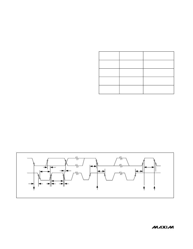
SDA
SCL
t
HD: STA
t
SU: DAT
t
HD: DAT
t
SU: STA
t
HD: STA
t
SU: STO
t
BUF
t
LOW
t
HIGH
t
R
t
F
START
CONDITION
REPEATED START
CONDITION
STOP
CONDITION
START
CONDITION
Figure 13. 2-Wire Serial Interface Timing Details
相關(guān)PDF資料 |
PDF描述 |
|---|---|
| MAX3301EEBA-T | CLAMP |
| MAX3301EETJ | CLAMP |
| MAX333A | Precision, Quad, SPDT, CMOS Analog Switch(MAX333的改進型,低導(dǎo)通電阻模擬開關(guān)) |
| MAX333 | High Speed Quad SPST Analog Switches(接通電阻175Ω,漏電流5nA,導(dǎo)通速率1000ns,單刀單擲模擬開關(guān)) |
| MAX334EJE | High Speed Quad SPST Analog Switch |
相關(guān)代理商/技術(shù)參數(shù) |
參數(shù)描述 |
|---|---|
| MAX3301EEBA | 制造商:Maxim Integrated Products 功能描述:USB ON-THE-GO TRANSCEIVER AND CHARG - Rail/Tube |
| MAX3301EEBA+ | 制造商:Maxim Integrated Products 功能描述:USB ON-THE-GO TRANSCEIVERS AND CHARGE PUMPS - Rail/Tube |
| MAX3301EEBA-T | 功能描述:USB 接口集成電路 RoHS:否 制造商:Cypress Semiconductor 產(chǎn)品:USB 2.0 數(shù)據(jù)速率: 接口類型:SPI 工作電源電壓:3.15 V to 3.45 V 工作電源電流: 最大工作溫度:+ 85 C 安裝風(fēng)格:SMD/SMT 封裝 / 箱體:WLCSP-20 |
| MAX3301EETI+ | 制造商:Maxim Integrated Products 功能描述:USB ON-THE-GO TRANSCEIVERS AND CHARGE PUMPS - Rail/Tube |
| MAX3301EETJ | 功能描述:USB 接口集成電路 RoHS:否 制造商:Cypress Semiconductor 產(chǎn)品:USB 2.0 數(shù)據(jù)速率: 接口類型:SPI 工作電源電壓:3.15 V to 3.45 V 工作電源電流: 最大工作溫度:+ 85 C 安裝風(fēng)格:SMD/SMT 封裝 / 箱體:WLCSP-20 |
發(fā)布緊急采購,3分鐘左右您將得到回復(fù)。