- 您現(xiàn)在的位置:買賣IC網(wǎng) > PDF目錄383346 > MAX2314EEI (MAXIM INTEGRATED PRODUCTS INC) CDMA IF VGAs and I/Q Demodulators with VCO and Synthesizer PDF資料下載
參數(shù)資料
| 型號: | MAX2314EEI |
| 廠商: | MAXIM INTEGRATED PRODUCTS INC |
| 元件分類: | 無繩電話/電話 |
| 英文描述: | CDMA IF VGAs and I/Q Demodulators with VCO and Synthesizer |
| 中文描述: | TELECOM, CELLULAR, BASEBAND CIRCUIT, PDSO28 |
| 封裝: | 0.150 INCH, 0.025 INCH PITCH, MO-137, QSOP-28 |
| 文件頁數(shù): | 15/22頁 |
| 文件大?。?/td> | 342K |
| 代理商: | MAX2314EEI |

M
CDMA IF VGAs and I/Q Demodulators
with VCO and Synthesizer
______________________________________________________________________________________
15
Synthesizer
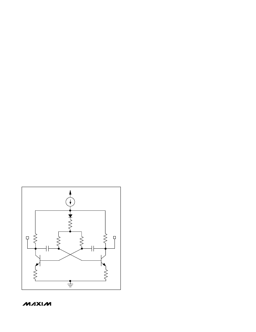
The VCO’s output frequency is controlled by an internal
phase-locked-loop (PLL) dual-modulus synthesizer.
The loop filter is off-chip to simplify loop design for
emerging applications. The tunable resonant network is
also off-chip for maximum Q and for system design
flexibility. The VCO output frequency is divided down to
the desired comparison frequency with the M counter.
The M counter consists of a 4-bit A swallow counter
and a 10-bit P counter. A reference signal is provided
from an external source and is divided down to the
comparison frequency with the R counter. The two
divided signals are compared with a three-state digital
phase-frequency detector. The phase-detector output
drives a charge pump as well as lock-detect logic and
turbocharge control logic. The charge pump output
(CP_OUT) pin is processed by the loop filter and drives
the tunable resonant network, altering the VCO fre-
quency and closing the loop.
Multimode applications are supported by two indepen-
dent programmable registers each for the M counter
(M1, M2), the R counter (R1, R2), and the charge-pump
output current magnitude (CP1, CP2). The DIVSEL (DS)
bit selects which set of registers is used. It can be over-
ridden by the MAX2310’s MODE pin or the MAX2312/
MAX2316’s DIVSEL pin. Programming these registers is
discussed in the
3-Wire Interface and Registers
sec-
tion.
When the part initially powers up or changes state, the
synthesizer acquisition time can be reduced by using
the Turbo feature, enabled by the TURBOCHARGE
(TC) control bit. Turbo functionality provides a larger
charge-pump current during acquisition mode. Once
the VCO frequency is acquired, the charge-pump out-
put current magnitude automatically returns to the pre-
programmed state to maintain loop stability and
minimize spurs in the VCO output signal.
The lock detect output indicates when the PLL is
locked with a logic high.
3-Wire Interface and Registers
The MAX2310 family incorporates a 3-wire interface for
synthesizer programming and device configuration
(Figure 5). The 3-wire interface consists of a clock,
data, and
ENABLE
. It controls the VCO dividers (M1
and M2), reference frequency dividers (R1 and R2),
and a 13-bit control register. The control register is
used to set up the operational modes (Table 4). The
input shift is 17 data bits long and requires a total of 18
clock bits (Figure 6). A single clock pulse is required
before enable drops low to initialize the data bus.
Whenever the M or R divide register value is pro-
grammed and downloaded, the control register must
also be subsequently updated. This prevents turbolock
from going active when not desired.
The
SHDN
control bit is notable because it differs from
the
SHDN
pin. When the
SHDN
control bit is low, the
registers and serial interface are left active, retaining
the values stored in the latches, while the rest of the
device is shut off. In contrast, the
SHDN
pin, when low,
shuts down everything, including the registers and seri-
al interface. See the functional diagram in Figure 7.
Registers
Figure 8 shows the programming logic. The 17-bit shift
register is programmed by clocking in data at the rising
edge of CLK. Before the shift register is able to accept
data, it must be initialized by driving it with at least one
full clock cycle at the CLK input with
EN
high (see
Figure 6). Pulling enable low will allow data to be
clocked into the shift register; pulling enable high loads
the register addressed by A0, A1, and A2, respectively
(Figure 8). Table 5 lists the power-on default values of
all registers. Table 6 lists the charge-pump current,
depending on CP0 and CP1.
800
μ
A
D1
R1
C
F
C
F
R
B
R
L
TANK+
TANK-
R
L
R
E
R
E
R
B
Figure 4. Voltage-Controlled Oscillators
相關(guān)PDF資料 |
PDF描述 |
|---|---|
| MAX2316EEI | CDMA IF VGAs and I/Q Demodulators with VCO and Synthesizer |
| MAX2310-MAX2316 | Quad 2-input positive-NAND buffers with open collector outputs 14-SOIC 0 to 70 |
| MAX2314 | Quad 2-input positive-NAND buffers with open collector outputs 14-SOIC 0 to 70 |
| MAX2374 | SiGe, Variable IIP3, Low-Noise Amplifier in UCSP Package |
| MAX2374EBT | SiGe, Variable IIP3, Low-Noise Amplifier in UCSP Package |
相關(guān)代理商/技術(shù)參數(shù) |
參數(shù)描述 |
|---|---|
| MAX2314EEI+ | 功能描述:調(diào)節(jié)器/解調(diào)器 RoHS:否 制造商:Texas Instruments 封裝 / 箱體:PVQFN-N24 封裝:Reel |
| MAX2314EEI+T | 功能描述:調(diào)節(jié)器/解調(diào)器 RoHS:否 制造商:Texas Instruments 封裝 / 箱體:PVQFN-N24 封裝:Reel |
| MAX2314EEI-T | 功能描述:調(diào)節(jié)器/解調(diào)器 RoHS:否 制造商:Texas Instruments 封裝 / 箱體:PVQFN-N24 封裝:Reel |
| MAX2314EVKIT | 功能描述:射頻開發(fā)工具 RoHS:否 制造商:Taiyo Yuden 產(chǎn)品:Wireless Modules 類型:Wireless Audio 工具用于評估:WYSAAVDX7 頻率: 工作電源電壓:3.4 V to 5.5 V |
| MAX2316EEI | 功能描述:調(diào)節(jié)器/解調(diào)器 RoHS:否 制造商:Texas Instruments 封裝 / 箱體:PVQFN-N24 封裝:Reel |
發(fā)布緊急采購,3分鐘左右您將得到回復(fù)。