- 您現(xiàn)在的位置:買賣IC網(wǎng) > PDF目錄383334 > MAX1999EEI (MAXIM INTEGRATED PRODUCTS INC) High-Efficiency, Quad Output, Main Power- Supply Controllers for Notebook Computers PDF資料下載
參數(shù)資料
| 型號: | MAX1999EEI |
| 廠商: | MAXIM INTEGRATED PRODUCTS INC |
| 元件分類: | 穩(wěn)壓器 |
| 英文描述: | High-Efficiency, Quad Output, Main Power- Supply Controllers for Notebook Computers |
| 中文描述: | DUAL SWITCHING CONTROLLER, 500 kHz SWITCHING FREQ-MAX, PDSO28 |
| 封裝: | 0.150 INCH, 0.025 INCH PITCH, QSOP-28 |
| 文件頁數(shù): | 30/32頁 |
| 文件大小: | 497K |
| 代理商: | MAX1999EEI |
第1頁第2頁第3頁第4頁第5頁第6頁第7頁第8頁第9頁第10頁第11頁第12頁第13頁第14頁第15頁第16頁第17頁第18頁第19頁第20頁第21頁第22頁第23頁第24頁第25頁第26頁第27頁第28頁第29頁當(dāng)前第30頁第31頁第32頁

M
High-Effic ienc y, Quad Output, Main Power-
S upply Controllers for Notebook Computers
30
______________________________________________________________________________________
PGND5). Avoid the introduction of AC currents into
the PGND3 and PGND5 ground planes. Run the
power plane ground currents on the top side only, if
possible.
Use a star ground connection on the power plane to
minimize the crosstalk between OUT3 and OUT5.
Keep the high-current paths short, especially at the
ground terminals. This practice is essential for sta-
ble, jitter-free operation.
Keep the power traces and load connections short.
This practice is essential for high efficiency. Using
thick copper PC boards (2oz vs. 1oz) can enhance
full-load efficiency by 1% or more. Correctly routing
PC board traces must be approached in terms of
fractions of centimeters, where a single milliohm of
excess trace resistance causes a measurable effi-
ciency penalty.
CS_ (MAX1777/MAX1977) / LX_ (MAX1999) and GND
connections to the synchronous rectifiers for current
limiting must be made using Kelvin sense connec-
tions to guarantee the current-limit accuracy. With 8-
pin SO MOSFETs, this is best done by routing power
to the MOSFETs from outside using the top copper
layer, while connecting CS_/LX_ traces inside (under-
neath) the MOSFETs.
When trade-offs in trace lengths must be made, it is
preferable to allow the inductor charging path to be
made longer than the discharge path. For example,
is better to allow some extra distance between the
input capacitors and the high-side MOSFET than to
allow distance between the inductor and the syn-
chronous rectifier or between the inductor and the
output filter capacitor.
Ensure that the OUT_ connection to C
OUT_
is short and
direct. However, in some cases it may be desirable to
deliberately introduce some trace length between the
OUT_ connector node and the output filter capacitor
(see the
Stability Considerations
section).
Route high-speed switching nodes (BST_, DH_, LX_,
and DL_) away from sensitive analog areas (REF,
ILIM_, and FB_). Use PGND3 and PGND5 as an EMI
shield to keep radiated switching noise away from the
IC’s feedback divider and analog bypass capacitors.
Make all pin-strap control input connections (
SKIP
,
ILIM_, etc.) to GND or V
CC
of the device.
Layout Proc edure
1) Place the power components first with ground ter-
minals adjacent (N2/N4 source, C
IN_
, C
OUT_
, D1
anode). If possible, make all these connections on
the top layer with wide, copper-filled areas.
2) Mount the controller IC adjacent to the synchronous
rectifier MOSFETs, preferably on the back side in
order to keep DH_, GND, and the DL_ gate drive
lines short and wide. The DL_ gate trace must be
short and wide measuring 50mils to 100mils wide if
the MOSFET is 1in from the controller device.
3) Group the gate-drive component (BST_ diode and
capacitor, V+ bypass capacitor) together near the
controller device.
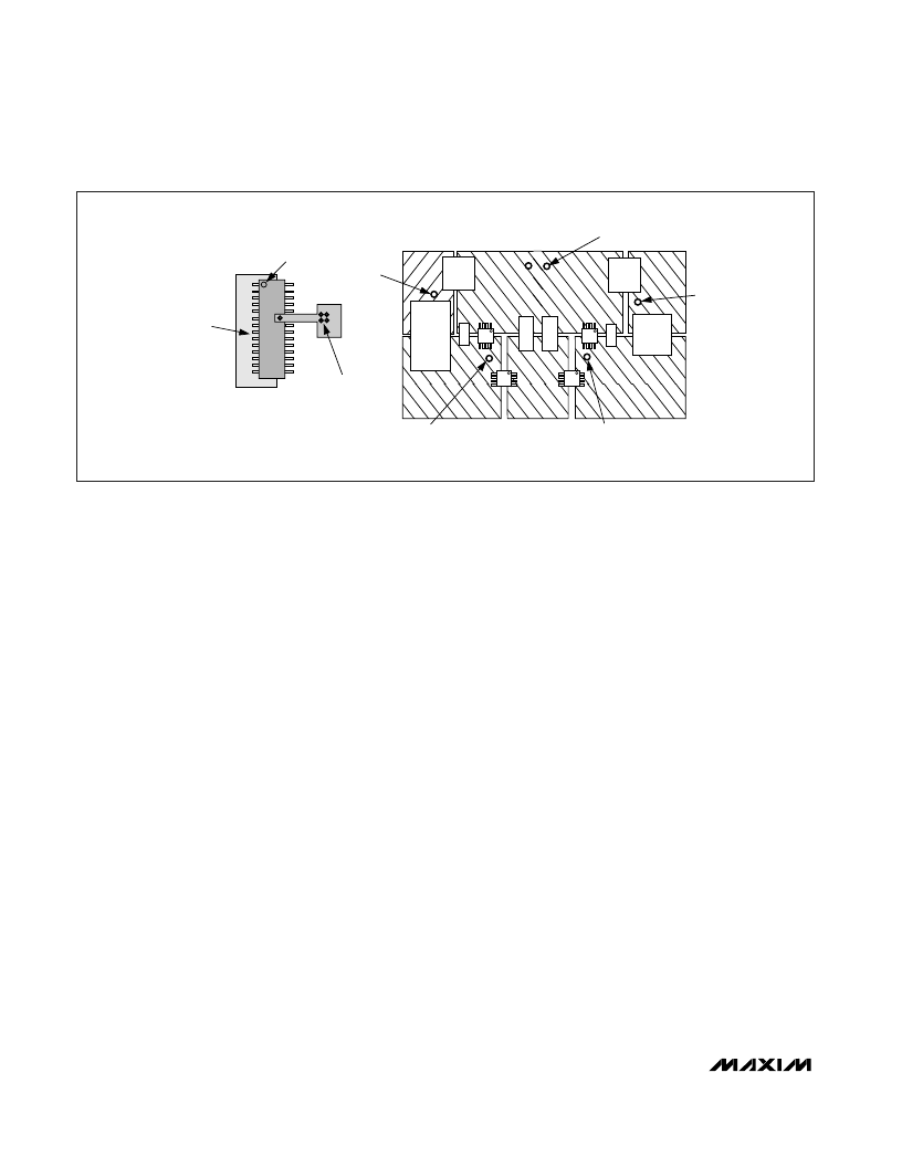
AGND
PGND
VIA TOOUT5
GROUND
OUT3
OUT5
VIA TOOUT3
VIA TOPGND
VIA TOLX5
V+
VIA TOLX3
USE AGND PLANE TO:
- BYPASS V
AND REF
- TERMINATE EXTERNAL FB
DIVIDER (IF USED)
- TERMINATE R
ILIM
(IF USED)
- PIN-STRAP CONTROL
INPUTS
USE PGND PLANE TO:
- BYPASS LDO_
- CONNECT PGND TOTHE TOPSIDE STAR GROUND
VIA BETWEEN POWER
AND ANALOG GROUND
VIAS TOGROUND
NOTE:
EXAMPLE SHOWN IS FOR DUAL N-CHANNEL MOSFET.
ANALOG GROUND
PLANE ON INNER LAYER
C4
C3
C1
N4
D
D
N2
C2
L1
L2
CONNECT PGND TOAGND
BENEATH THE CONTROLLER AT
ONE POINT ONLY AS SHOWN.
N3
N1
Figure 13. PC Board Layout Example
相關(guān)PDF資料 |
PDF描述 |
|---|---|
| MAX1778 | 32-Bit Digital Signal Controller with ROM 100-LQFP -40 to 85 |
| MAX1880 | Quad-Output TFT LCD DC-DC Converters with Buffer |
| MAX1881 | Quad-Output TFT LCD DC-DC Converters with Buffer |
| MAX1882 | Quad-Output TFT LCD DC-DC Converters with Buffer |
| MAX1883 | Quad-Output TFT LCD DC-DC Converters with Buffer |
相關(guān)代理商/技術(shù)參數(shù) |
參數(shù)描述 |
|---|---|
| MAX1999EEI+ | 功能描述:DC/DC 開關(guān)控制器 Quad Out Main Power Supply Controller RoHS:否 制造商:Texas Instruments 輸入電壓:6 V to 100 V 開關(guān)頻率: 輸出電壓:1.215 V to 80 V 輸出電流:3.5 A 輸出端數(shù)量:1 最大工作溫度:+ 125 C 安裝風(fēng)格: 封裝 / 箱體:CPAK |
| MAX1999EEI+T | 功能描述:DC/DC 開關(guān)控制器 Quad Out Main Power Supply Controller RoHS:否 制造商:Texas Instruments 輸入電壓:6 V to 100 V 開關(guān)頻率: 輸出電壓:1.215 V to 80 V 輸出電流:3.5 A 輸出端數(shù)量:1 最大工作溫度:+ 125 C 安裝風(fēng)格: 封裝 / 箱體:CPAK |
| MAX1999EEI-T | 功能描述:DC/DC 開關(guān)控制器 RoHS:否 制造商:Texas Instruments 輸入電壓:6 V to 100 V 開關(guān)頻率: 輸出電壓:1.215 V to 80 V 輸出電流:3.5 A 輸出端數(shù)量:1 最大工作溫度:+ 125 C 安裝風(fēng)格: 封裝 / 箱體:CPAK |
| MAX1999EVKIT | 功能描述:DC/DC 開關(guān)控制器 Evaluation Kit for the MAX1777 MAX1977 MAX1999 RoHS:否 制造商:Texas Instruments 輸入電壓:6 V to 100 V 開關(guān)頻率: 輸出電壓:1.215 V to 80 V 輸出電流:3.5 A 輸出端數(shù)量:1 最大工作溫度:+ 125 C 安裝風(fēng)格: 封裝 / 箱體:CPAK |
| MAX199ACAI | 功能描述:模數(shù)轉(zhuǎn)換器 - ADC RoHS:否 制造商:Texas Instruments 通道數(shù)量:2 結(jié)構(gòu):Sigma-Delta 轉(zhuǎn)換速率:125 SPs to 8 KSPs 分辨率:24 bit 輸入類型:Differential 信噪比:107 dB 接口類型:SPI 工作電源電壓:1.7 V to 3.6 V, 2.7 V to 5.25 V 最大工作溫度:+ 85 C 安裝風(fēng)格:SMD/SMT 封裝 / 箱體:VQFN-32 |
發(fā)布緊急采購,3分鐘左右您將得到回復(fù)。