- 您現(xiàn)在的位置:買賣IC網(wǎng) > PDF目錄383344 > MAX1994ETM (MAXIM INTEGRATED PRODUCTS INC) Dual Step-Down Controllers Plus Linear- Regulator Controller for Notebook Computers PDF資料下載
參數(shù)資料
| 型號: | MAX1994ETM |
| 廠商: | MAXIM INTEGRATED PRODUCTS INC |
| 元件分類: | 穩(wěn)壓器 |
| 英文描述: | Dual Step-Down Controllers Plus Linear- Regulator Controller for Notebook Computers |
| 中文描述: | DUAL SWITCHING CONTROLLER, 1000 kHz SWITCHING FREQ-MAX, CQCC48 |
| 封裝: | 7 X 7 MM, 0.80 MM HEIGHT, THIN, QFN-48 |
| 文件頁數(shù): | 31/49頁 |
| 文件大小: | 983K |
| 代理商: | MAX1994ETM |
第1頁第2頁第3頁第4頁第5頁第6頁第7頁第8頁第9頁第10頁第11頁第12頁第13頁第14頁第15頁第16頁第17頁第18頁第19頁第20頁第21頁第22頁第23頁第24頁第25頁第26頁第27頁第28頁第29頁第30頁當(dāng)前第31頁第32頁第33頁第34頁第35頁第36頁第37頁第38頁第39頁第40頁第41頁第42頁第43頁第44頁第45頁第46頁第47頁第48頁第49頁

M
Dual Step-Down Controllers Plus Linear-
Regulator Controller for Notebook Computers
______________________________________________________________________________________
31
DC output accuracy specifications for BUCK2 refer to
the threshold of the error comparator. When the induc-
tor is in continuous conduction, BUCK2 output voltage
has a DC regulation level higher than the trip level by
50% of the ripple. In discontinuous conduction
(SKP2/
SDN
= high, light-loaded), BUCK2 output volt-
age has a DC regulation level higher than the error-
comparator threshold by approximately 1.5% due to
slope compensation.
Note that BUCK1 automatically enters forced-PWM
mode during all output voltage transitions and stays in
forced-PWM mode until the transition is completed and
for 32 clock cycles thereafter. The reason for that is the
forced-PWM operation provides current sinking capa-
bility required during output-voltage transitions.
Linear-Regulator Controller
The linear-regulator controller of the MAX1816/MAX1994
is an analog gain block with an open-drain N-channel
output. It drives an external PNP pass transistor with a
220
base-to-emitter resistor (Figure 1). The controller
is guaranteed to provide at least 20mA sink current. The
linear regulator is typically used to provide a
1.2V/500mA VID logic supply. The controller is designed
to be stable with an output capacitor of 10μF or more.
The output voltage can be adjusted with a resistive volt-
age-divider between the linear regulator output and
analog ground with the center tap connected to LINFB.
The set point of LINFB is 1.0V. The regulator is enabled
when LIN/
SDN
is high. As soon as LINFB is in regula-
tion, the open-drain power-good output LINGOOD goes
high after a 1ms (min) delay. When the output goes out
of regulation or LIN/
SDN
goes low, LINGOOD is forced
low within approximately 10μs.
The 1ms (min) LINGOOD delay is necessary to allow
the PLLs in the CPU to power up and stabilize before
turning on the main regulator. The delay time is com-
puted based on 1024 R
TIME
clock cycles. As such, the
delay varies based on the R
TIME
period.
MOSFET Gate Drivers (DH_, DL_)
The DH_ and DL_ drivers are optimized for driving mod-
erate-sized high-side and larger low-side power
MOSFETs. This is consistent with the low duty factor
seen in the notebook CPU environment, where a large
V
IN
- V
OUT
_ differential exists. Two adaptive dead-time
circuits monitor the DH_ and DL_ outputs and prevent
the opposite side FET from turning on until DL_ or DH_ is
fully off. There must be a low-resistance, low-inductance
path from the DL_ and DH_ drivers to the MOSFET gates
for the adaptive dead-time circuits to work properly.
Otherwise, the sense circuitry in the MAX1816/MAX1994
interprets the MOSFET gate as
“
off
”
while there is actual-
ly still charge left on the gate. Use very short, wide traces
measuring 10 to 20 squares (50 mils to 100 mils wide if
the MOSFET is 1in from the MAX1816/MAX1994).
The internal pulldown transistor that drives DL_ low is
robust, with a very low pulldown resistance. For DL1,
this resistance is 0.35
(typ), while the resistance for
DL2 is slightly higher at 0.7
(typ). This helps prevent
DL_ from being pulled up during the fast rise-time of
the inductor node, due to capacitive coupling from the
drain to the gate of the low-side synchronous-rectifier
MOSFET. However, for high-current applications, some
combinations of high- and low-side FETs can cause
excessive gate-drain coupling, which can lead to effi-
ciency-killing, EMI-producing shoot-through currents.
This is often remedied by adding a resistor in series
with BST_, which increases the turn-on time of the high-
side FET without degrading the turn-off time (Figure 8).
LX_
+5V
V
BATT
5
TYP
DH_
BST_
MAX1816
MAX1994
Figure 8. Reducing the Switching-Node Rise Time
I
I
LOAD
= I
PEAK
/2
ON-TIME
0
TIME
I
PEAK
L
V
BATT
- V
OUT
i
t
=
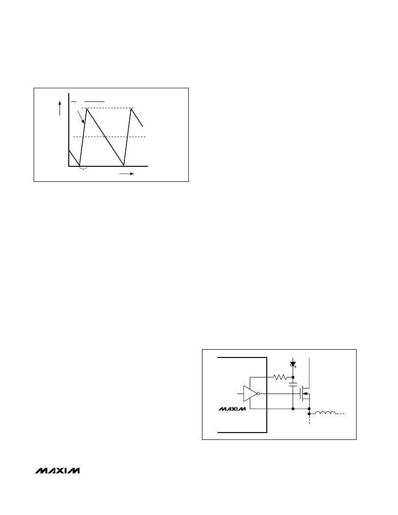
Figure 7. Pulse-Skipping/Discontinuous Crossover Point
相關(guān)PDF資料 |
PDF描述 |
|---|---|
| MAX1816 | Replaced by TMS320VC5506 : Digital Signal Processors 144-LQFP |
| MAX1816ETM | Replaced by TMS320VC5506 : Digital Signal Processors 144-LQFP |
| MAX199AEWI | Fixed-Point Digital Signal Processor 532-FCBGA |
| MAX199AMYI | Circular Connector; No. of Contacts:18; Series:MS27505; Body Material:Aluminum; Connecting Termination:Crimp; Connector Shell Size:15; Circular Contact Gender:Socket; Circular Shell Style:Box Mount Receptacle RoHS Compliant: No |
| MAX199ACAI | Multi-Range (【4V, 【2V, +4V, +2V), +5V Supply, 12-Bit DAS with 8+4 Bus Interface |
相關(guān)代理商/技術(shù)參數(shù) |
參數(shù)描述 |
|---|---|
| MAX1994ETM+ | 功能描述:DC/DC 開關(guān)控制器 Integrated Circuits (ICs) RoHS:否 制造商:Texas Instruments 輸入電壓:6 V to 100 V 開關(guān)頻率: 輸出電壓:1.215 V to 80 V 輸出電流:3.5 A 輸出端數(shù)量:1 最大工作溫度:+ 125 C 安裝風(fēng)格: 封裝 / 箱體:CPAK |
| MAX1994ETM+T | 功能描述:DC/DC 開關(guān)控制器 Integrated Circuits (ICs) RoHS:否 制造商:Texas Instruments 輸入電壓:6 V to 100 V 開關(guān)頻率: 輸出電壓:1.215 V to 80 V 輸出電流:3.5 A 輸出端數(shù)量:1 最大工作溫度:+ 125 C 安裝風(fēng)格: 封裝 / 箱體:CPAK |
| MAX1994ETM-T | 功能描述:DC/DC 開關(guān)控制器 RoHS:否 制造商:Texas Instruments 輸入電壓:6 V to 100 V 開關(guān)頻率: 輸出電壓:1.215 V to 80 V 輸出電流:3.5 A 輸出端數(shù)量:1 最大工作溫度:+ 125 C 安裝風(fēng)格: 封裝 / 箱體:CPAK |
| MAX1994EVKIT | 功能描述:DC/DC 開關(guān)控制器 Evaluation Kit for the MAX1816 MAX1980 MAX1994 RoHS:否 制造商:Texas Instruments 輸入電壓:6 V to 100 V 開關(guān)頻率: 輸出電壓:1.215 V to 80 V 輸出電流:3.5 A 輸出端數(shù)量:1 最大工作溫度:+ 125 C 安裝風(fēng)格: 封裝 / 箱體:CPAK |
| MAX1995EGI | 功能描述:顯示驅(qū)動器和控制器 RoHS:否 制造商:Panasonic Electronic Components 工作電源電壓:2.7 V to 5.5 V 最大工作溫度: 安裝風(fēng)格:SMD/SMT 封裝 / 箱體:QFN-44 封裝:Reel |
發(fā)布緊急采購,3分鐘左右您將得到回復(fù)。