- 您現(xiàn)在的位置:買賣IC網(wǎng) > PDF目錄383340 > MAX1909 (Maxim Integrated Products, Inc.) Multichemistry Battery Charger with Automatic System Power Selector PDF資料下載
參數(shù)資料
| 型號(hào): | MAX1909 |
| 廠商: | Maxim Integrated Products, Inc. |
| 英文描述: | Multichemistry Battery Charger with Automatic System Power Selector |
| 中文描述: | 多種化學(xué)類型電池充電器,自動(dòng)選擇系統(tǒng)電源 |
| 文件頁數(shù): | 26/29頁 |
| 文件大?。?/td> | 551K |
| 代理商: | MAX1909 |
第1頁第2頁第3頁第4頁第5頁第6頁第7頁第8頁第9頁第10頁第11頁第12頁第13頁第14頁第15頁第16頁第17頁第18頁第19頁第20頁第21頁第22頁第23頁第24頁第25頁當(dāng)前第26頁第27頁第28頁第29頁

M
Multichemistry Battery Charger with Automatic
System Power Selector
26
______________________________________________________________________________________
mately 15V. Switching losses in the high-side MOSFET
can become an insidious heat problem when maximum
AC adapter voltages are applied, due to the squared
term in the CV
2
f switching-loss equation. If the high-
side MOSFET that was chosen for adequate RDS(ON)
at low supply voltages becomes extraordinarily hot
when subjected to V
DCIN(MAX),
then choose a MOSFET
with lower losses. Calculating the power dissipation in
P1 due to switching losses is difficult since it must allow
for difficult quantifying factors that influence the turn-on
and turn-off times. These factors include the internal
gate resistance, gate charge, threshold voltage, source
inductance, and PC board layout characteristics. The
following switching-loss calculation provides only a
very rough estimate and is no substitute for breadboard
evaluation, preferably including a verification using a
thermocouple mounted on P1:
where CRSS is the reverse transfer capacitance of P1,
and I
GATE
is the peak gate-drive source/sink current.
For the low-side MOSFET (N1), the worst-case power
dissipation always occurs at maximum input voltage:
Choose a Schottky diode (D1, Figure 2) having a for-
ward voltage low enough to prevent the N1 MOSFET
body diode from turning on during the dead time. As a
general rule, a diode with a DC current rating equal to
1/3rd the load current is sufficient. This diode is option-
al and can be removed if efficiency is not critical.
Inductor Selection
The charge current, ripple, and operating frequency
(off-time) determine the inductor characteristics.
Inductor L1 must have a saturation current rating of at
least the maximum charge current plus 1/2 of the ripple
current (
IL):
I
SAT
= I
CHG
+ (1/2)
IL
The ripple current is determined by:
IL = V
BATT
t
OFF
/ L
where:
t
OFF
= 2.5us (V
DCIN
- V
BATT
) / V
DCIN
for
V
BATT
< 0.88 V
DCIN
or:
t
OFF
= 0.3us for V
BATT
> 0.88 V
DCIN
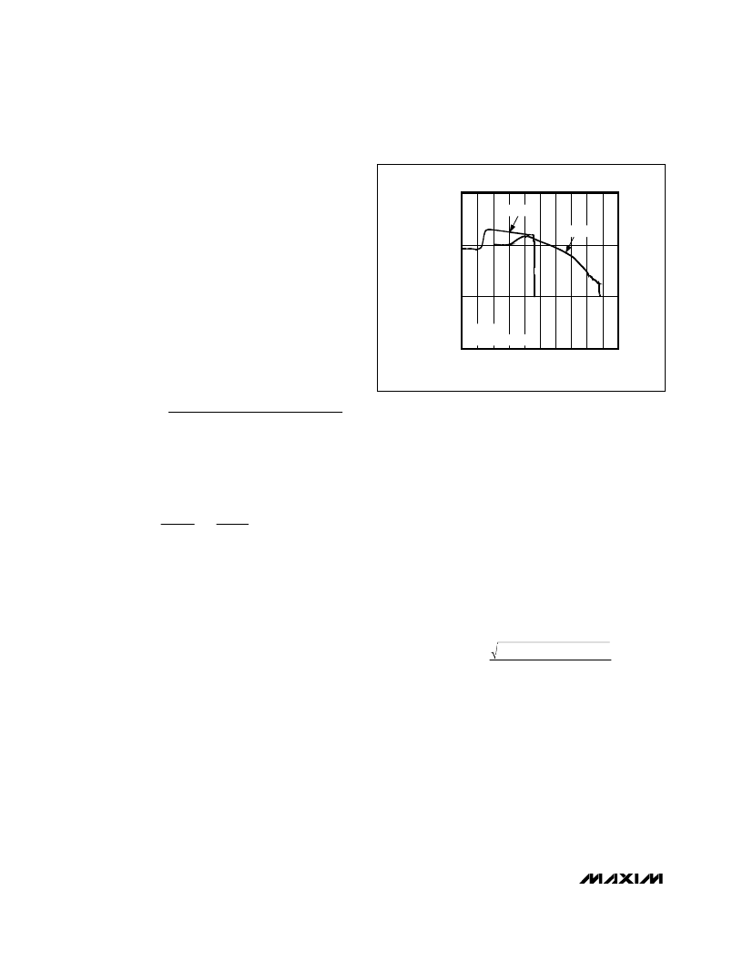
Figure 11 illustrates the variation of the ripple current
vs. battery voltage when the circuit is charging at 3A
with a fixed input voltage of 19V.
Higher inductor values decrease the ripple current.
Smaller inductor values require high-saturation current
capabilities and degrade efficiency. Designs that set
LIR =
IL/I
CHG
= 0.3 usually result in a good balance
between inductor size and efficiency.
Input Capacitor Selection
The input capacitor must meet the ripple current
requirement (I
RMS
) imposed by the switching currents.
Nontantalum chemistries (ceramic, aluminum, or OS-
CON) are preferred due to their resilience to power-up
surge currents.
The input capacitors should be sized so that the
temperature rise due to ripple current in continuous
conduction does not exceed about 10
°
C. The
maximum ripple current occurs at 50% duty factor or
V
DCIN
= 2
V
BATT
, which equates to 0.5
I
CHG
. If the
application of interest does not achieve the maximum
value, size the input capacitors according to the
worst-case conditions.
Output Capacitor Selection
The output capacitor absorbs the inductor ripple cur-
rent and must tolerate the surge current delivered from
the battery when it is initially plugged into the charger.
I
I
V
V
V
V
RMS
CHG
BATT
DCIN
BATT
DCIN
=
(
)
PD N
V
V
I
R
BATT
DCIN
LOAD
2
DS ON
(
(
)
)
1
1
2
=
×
PD P
Switching
V
C
I
f
I
DCIN MAX
(
RSS
SW
LOAD
GATE
(
_
)
)
1
2
2
=
×
×
×
0
1.0
0.5
1.5
8
10
11
12
13
9
14
15
16
17
18
V
BATT
(V)
R
V
DCIN
= 19V
VCTL = ICTL = LDO
3 CELLS
4 CELLS
Figure 11. Ripple Current vs. Battery Voltage
相關(guān)PDF資料 |
PDF描述 |
|---|---|
| MAX1909ETI | Multichemistry Battery Charger with Automatic System Power Selector |
| MAX190AENG | Low-Power, 12-Bit Sampling ADCs with Internal Reference and Power-Down |
| MAX191BMRG | Low-Power, 12-Bit Sampling ADCs with Internal Reference and Power-Down |
| MAX190 | Low-Power, 12-Bit Sampling ADCs with Internal Reference and Power-Down |
| MAX190BENG | Low-Power, 12-Bit Sampling ADCs with Internal Reference and Power-Down |
相關(guān)代理商/技術(shù)參數(shù) |
參數(shù)描述 |
|---|---|
| MAX1909ETI | 功能描述:電池管理 RoHS:否 制造商:Texas Instruments 電池類型:Li-Ion 輸出電壓:5 V 輸出電流:4.5 A 工作電源電壓:3.9 V to 17 V 最大工作溫度:+ 85 C 最小工作溫度:- 40 C 封裝 / 箱體:VQFN-24 封裝:Reel |
| MAX1909ETI+ | 功能描述:電池管理 Multichemistry Battery Chargers RoHS:否 制造商:Texas Instruments 電池類型:Li-Ion 輸出電壓:5 V 輸出電流:4.5 A 工作電源電壓:3.9 V to 17 V 最大工作溫度:+ 85 C 最小工作溫度:- 40 C 封裝 / 箱體:VQFN-24 封裝:Reel |
| MAX1909ETI+T | 功能描述:電池管理 Multichemistry Battery Chargers RoHS:否 制造商:Texas Instruments 電池類型:Li-Ion 輸出電壓:5 V 輸出電流:4.5 A 工作電源電壓:3.9 V to 17 V 最大工作溫度:+ 85 C 最小工作溫度:- 40 C 封裝 / 箱體:VQFN-24 封裝:Reel |
| MAX1909ETI-T | 功能描述:電池管理 RoHS:否 制造商:Texas Instruments 電池類型:Li-Ion 輸出電壓:5 V 輸出電流:4.5 A 工作電源電壓:3.9 V to 17 V 最大工作溫度:+ 85 C 最小工作溫度:- 40 C 封裝 / 箱體:VQFN-24 封裝:Reel |
| MAX1909EVKIT | 功能描述:電池管理 Evaluation Kit for the MAX1909 RoHS:否 制造商:Texas Instruments 電池類型:Li-Ion 輸出電壓:5 V 輸出電流:4.5 A 工作電源電壓:3.9 V to 17 V 最大工作溫度:+ 85 C 最小工作溫度:- 40 C 封裝 / 箱體:VQFN-24 封裝:Reel |
發(fā)布緊急采購(gòu),3分鐘左右您將得到回復(fù)。