- 您現(xiàn)在的位置:買賣IC網(wǎng) > PDF目錄65800 > MA4PBL027 SILICON, PIN DIODE PDF資料下載
參數(shù)資料
| 型號: | MA4PBL027 |
| 元件分類: | PIN二極管 |
| 英文描述: | SILICON, PIN DIODE |
| 封裝: | CASE ODS-1302, 2 PIN |
| 文件頁數(shù): | 2/5頁 |
| 文件大小: | 309K |
| 代理商: | MA4PBL027 |
HMICTM Silicon Beam-Lead PIN Diodes
M/A-COM Inc. and its affiliates reserve the right to make changes to the
product(s) or information contained herein without notice. M/A-COM makes
no warranty, representation or guarantee regarding the suitability of its
products for any particular purpose, nor does M/A-COM assume any liability
whatsoever arising out of the use or application of any product(s) or
information.
North America Tel: 800.366.2266 / Fax: 978.366.2266
Europe Tel: 44.1908.574.200 / Fax: 44.1908.574.300
Asia/Pacific Tel: 81.44.844.8296 / Fax: 81.44.844.8298
Visit www.macom.com for additional data sheets and product information.
2
V1
MA4PBL027
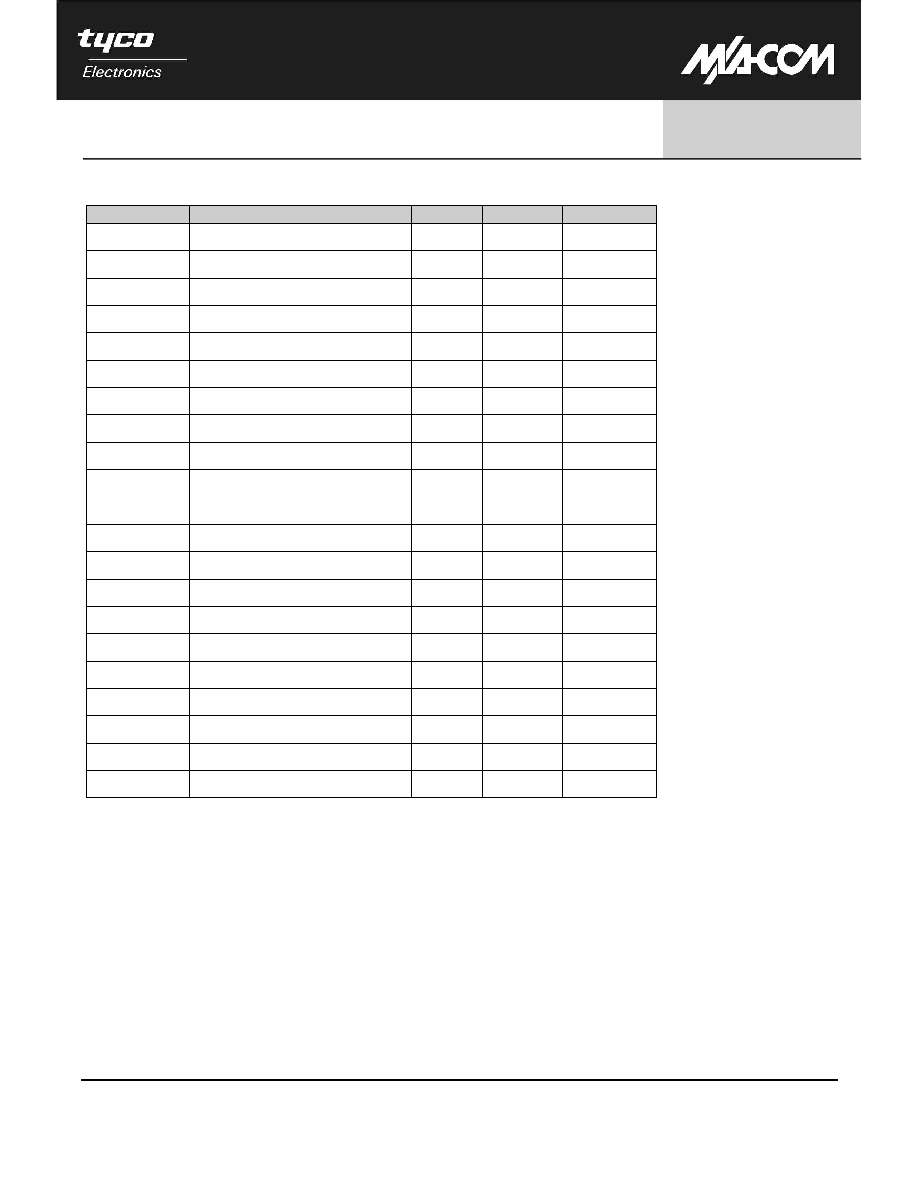
Electrical Specifications at +25 °C
Symbol
Conditions
Units
Typ.
Max.
CT
0 V, 1 MHz
2
pF
0.048
CT
-3 V, 1 MHz
2
pF
0.039
CT
-10 V, 1 MHz
2
pF
0.033
0.040
CT
-40 V, 1 MHz
2
pF
0.030
0.040
CT
0 V, 100 MHz
2,4
pF
0.043
CT
-3 V, 100 MHz
2,4
pF
0.033
CT
-10V, 100 MHz
2,4
pF
0.031
CT
-40V, 100 MHz
2,4
pF
0.027
CT
0 V, 1 GHz
2,4
pF
0.039
CT
-3 V, 1 GHz
2,4
pF
0.032
CT
-10 V, 1 GHz
2,4
pF
0.029
CT
-40 V, 1 GHz
2,4
pF
0.026
RS
10 mA, 100 MHz
3,4
3.8
RS
20 mA, 100 MHz
3,4
3.0
RS
10 mA, 1 GHz
3,4
3.5
RS
20 mA, 1 GHz
3,4
2.8
VF
20 mA
V
0.917
1.1
VR
-10
A
V
110
IR
-40 V
nA
1.0
IR
-90 V
uA
-
10.0
TL
+10 mA / -6 mA
ns
110
2. Total capacitance,
CT, is equivalent to the sum of Junction Capacitance ,Cj, and Parasitic Capacitance, Cpar.
3. Series resistance RS is equivalent to the total diode resistance : Rs = Rj ( Junction Resistance) + Rc ( Ohmic Resistance)
4. Rs and CT are measured on an HP4291A Impedance Analyzer with die mounted in an ODS-186 package with conductive silver epoxy.
NOTES:
Die Handling
All semiconductor chips should be handled with care
to avoid damage or contamination from perspiration
and skin oils. The use of plastic tipped tweezers or
vacuum
pickups
is
strongly
recommended
for
individual components. Bulk handling should insure
that abrasion and mechanical shock are minimized.
Die Bonding
These devices were designed to be inserted onto
hard or soft substrates. Recommended methods of
attachment include thermocompression bonding, par-
allel-gap welding, and electrically conductive silver epoxy.
See
Application
Note
M541,
“Bonding
and
Handling Procedures for Chip Diode Devices” for
More Detailed Assembly Instructions.
相關PDF資料 |
PDF描述 |
|---|---|
| MA4ST1320-1279T | 55 pF, 12 V, SILICON, HYPERABRUPT VARIABLE CAPACITANCE DIODE |
| MA4ST350-287 | S BAND, 11.8 pF, 12 V, SILICON, HYPERABRUPT VARIABLE CAPACITANCE DIODE |
| MA4ST340-287 | S BAND, 18.5 pF, 12 V, SILICON, HYPERABRUPT VARIABLE CAPACITANCE DIODE |
| MA4X7130G | MIXER DIODE |
| MA652 | 20 A, 200 V, SILICON, RECTIFIER DIODE, TO-220AB |
相關代理商/技術參數(shù) |
參數(shù)描述 |
|---|---|
| MA4PH151 | 制造商:MA-COM 制造商全稱:M/A-COM Technology Solutions, Inc. 功能描述:Surface Mount Plastic PIN Diodes |
| MA4PH151-139T | 制造商:M/A-COM Technology Solutions 功能描述:AXIAL LEAD PIN DIODE - Tape and Reel 制造商:M/A-COM Technology Solutions 功能描述:RF PIN DIODE |
| MA4PH152-1072 | 制造商:M/A-COM Technology Solutions 功能描述:SPECIAL PRODUCT - Bulk |
| MA4PH152-1072T | 制造商:M/A-COM Technology Solutions 功能描述:SPECIAL PRODUCT - Tape and Reel |
| MA4PH235 | 制造商:M/A-COM TECHNOLOGY SOLUTI 功能描述: 制造商:MA-COM 功能描述: |
發(fā)布緊急采購,3分鐘左右您將得到回復。