- 您現(xiàn)在的位置:買賣IC網(wǎng) > PDF目錄224146 > M48T128V (意法半導(dǎo)體) 3.3V-5V 1 Mbit 128Kb x8 TIMEKEEPER SRAM PDF資料下載
參數(shù)資料
| 型號(hào): | M48T128V |
| 廠商: | 意法半導(dǎo)體 |
| 元件分類: | SRAM |
| 英文描述: | 3.3V-5V 1 Mbit 128Kb x8 TIMEKEEPER SRAM |
| 中文描述: | 3.3 - 5V的1兆位的SRAM 128KB的x8計(jì)時(shí)器 |
| 文件頁數(shù): | 3/22頁 |
| 文件大小: | 340K |
| 代理商: | M48T128V |
11/22
M48T128Y, M48T128V*
CLOCK OPERATIONS
Reading the Clock
Updates to the TIMEKEEPER registers should
be halted before clock data is read to prevent
reading data in transition. The BiPORT TIME-
KEEPER cells in the RAM array are only data reg-
isters and not the actual clock counters, so
updating the registers can be halted without dis-
turbing the clock itself.
Updating is halted when a '1' is written to the
READ Bit, D6 in the Control Register (1FFF8h). As
long as a '1' remains in that position, updating is
halted. After a halt is issued, the registers reflect
the count; that is, the day, date, and time that were
current at the moment the halt command was is-
sued. All of the TIMEKEEPER registers are updat-
ed simultaneously. A halt will not interrupt an
update in progress. Updating is within a second af-
ter the bit is reset to a '0.'
Setting the Clock
Bit D7 of the Control Register (1FFF8h) is the
WRITE Bit. Setting the WRITE Bit to a '1,' like the
READ Bit, halts updates to the TIMEKEEPER reg-
isters. The user can then load them with the cor-
rect day, date, and time data in 24 hour BCD
format (see Table 5., page 11). Resetting the
WRITE Bit to a '0' then transfers the values of all
time registers 1FFFFh-1FFF9h to the actual TIME-
KEEPER counters and allows normal operation to
resume. After the WRITE Bit is reset, the next
clock update will occur one second later.
Stopping and Starting the Oscillator
The oscillator may be stopped at any time. If the
device is going to spend a significant amount of
time on the shelf, the oscillator can be turned off to
minimize current drain on the battery. The STOP
Bit is located at Bit D7 within 1FFF9h. Setting it to
a '1' stops the oscillator. The M48T128Y/V is
shipped from STMicroelectronics with the STOP
Bit set to a '1.' When reset to a '0,' the M48T128Y/
V oscillator starts after one second.
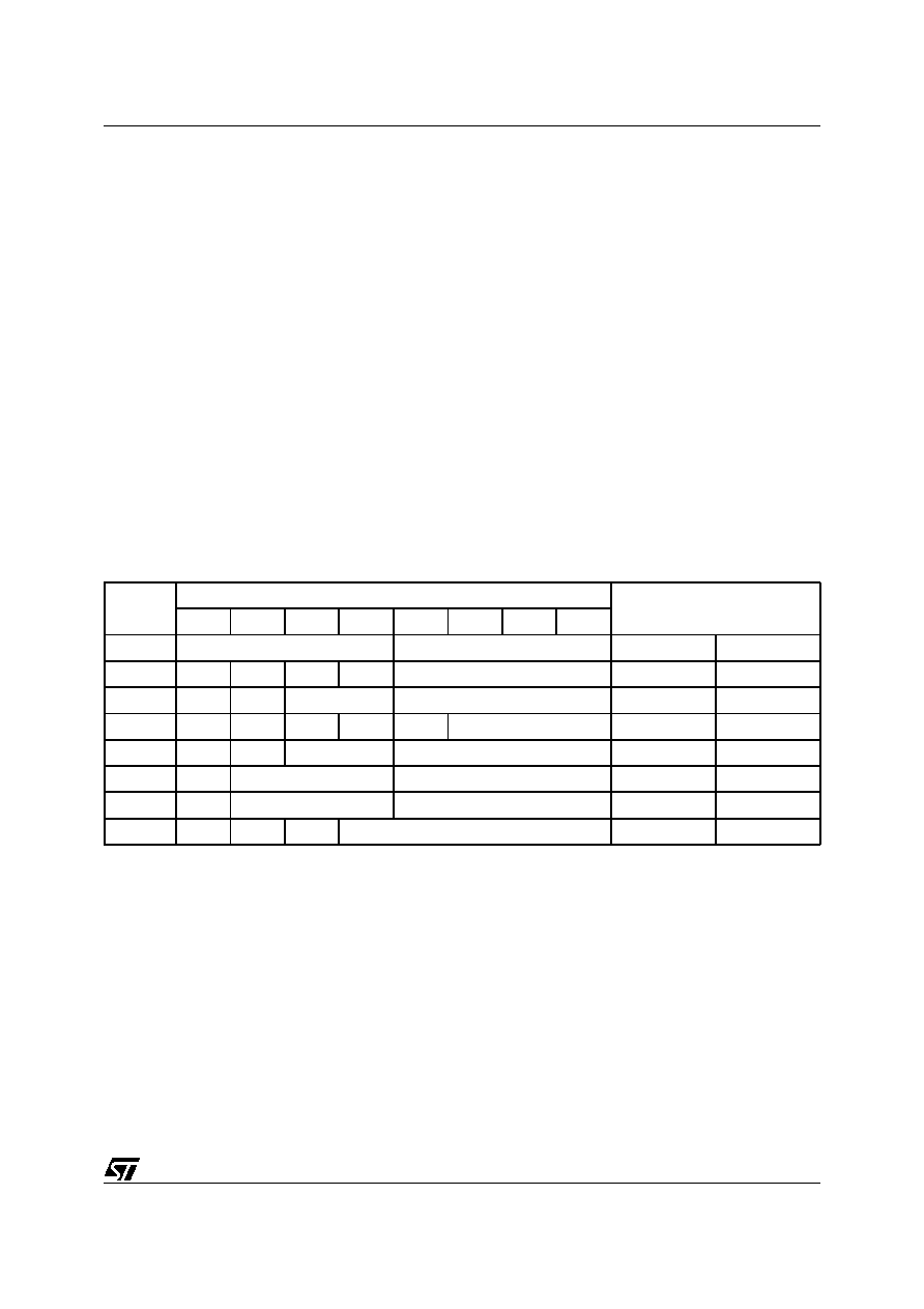
Table 5. Register Map
Keys: S = SIGN Bit
R = READ Bit
W = WRITE Bit
ST = STOP Bit
0 = Must be set to '0'
Z = '0' and are Read only
Y = '1' or '0'
Address
Data
Function/Range
BCD Format
D7
D6
D5
D4
D3
D2
D1
D0
1FFFFh
10 Years
Year
00-99
1FFFEh
0
10 M
Month
01-12
1FFFDh
0
10 Date
Date
01-31
1FFFCh
0
FT
0
Day
01-07
1FFFBh
0
10 Hours
Hours
00-23
1FFFAh
0
10 Minutes
Minutes
00-59
1FFF9h
ST
10 Seconds
Seconds
00-59
1FFF8h
W
R
S
Calibration
Control
相關(guān)PDF資料 |
PDF描述 |
|---|---|
| M48T12 | 16 Kbit 2Kb x8 TIMEKEEPER[ SRAM |
| M48T12-150PC1 | 16 Kbit 2Kb x8 TIMEKEEPER[ SRAM |
| M48T12-200PC1 | 16 Kbit 2Kb x8 TIMEKEEPER[ SRAM |
| M48T12-70PC1 | 16 Kbit 2Kb x8 TIMEKEEPER[ SRAM |
| M4R16XBJFREQ | CRYSTAL OSCILLATOR, CLOCK, 19.44 MHz - 200 MHz, PECL OUTPUT |
相關(guān)代理商/技術(shù)參數(shù) |
參數(shù)描述 |
|---|---|
| M48T128V-70PM1 | 制造商:STMICROELECTRONICS 制造商全稱:STMicroelectronics 功能描述:3.3V-5V 1 Mbit 128Kb x8 TIMEKEEPER SRAM |
| M48T128V-70PM1TR | 制造商:STMICROELECTRONICS 制造商全稱:STMicroelectronics 功能描述:3.3V-5V 1 Mbit 128Kb x8 TIMEKEEPER SRAM |
| M48T128V-80PM1 | 制造商:STMICROELECTRONICS 制造商全稱:STMicroelectronics 功能描述:5.0 or 3.3 V, 1 Mbit (128 Kb x 8) TIMEKEEPER?? SRAM |
| M48T128V-85PM1 | 制造商:STMICROELECTRONICS 制造商全稱:STMicroelectronics 功能描述:3.3V-5V 1 Mbit 128Kb x8 TIMEKEEPER SRAM |
| M48T128V-85PM1TR | 制造商:STMICROELECTRONICS 制造商全稱:STMicroelectronics 功能描述:3.3V-5V 1 Mbit 128Kb x8 TIMEKEEPER SRAM |
發(fā)布緊急采購,3分鐘左右您將得到回復(fù)。