- 您現(xiàn)在的位置:買賣IC網(wǎng) > PDF目錄224146 > M40SZ100WMQ (意法半導(dǎo)體) 5V or 3V NVRAM SUPERVISOR FOR LPSRAM PDF資料下載
參數(shù)資料
| 型號: | M40SZ100WMQ |
| 廠商: | 意法半導(dǎo)體 |
| 英文描述: | 5V or 3V NVRAM SUPERVISOR FOR LPSRAM |
| 中文描述: | 5V或3V的LPSRAM NVRAM中督導(dǎo)員 |
| 文件頁數(shù): | 4/19頁 |
| 文件大小: | 285K |
| 代理商: | M40SZ100WMQ |
M40SZ100Y, M40SZ100W
12/19
Battery Low Pin
The M40SZ100Y/W automatically performs bat-
tery voltage monitoring upon power-up, and at fac-
tory-programmed time intervals of at least 24
hours. The Battery Low (BL) pin will be asserted if
the battery voltage is found to be less than approx-
imately 2.5V. The BL pin will remain asserted until
completion of battery replacement and subse-
quent battery low monitoring tests, either during
the next power-up sequence or the next scheduled
24-hour interval.
If a battery low is generated during a power-up se-
quence, this indicates that the battery is below
2.5V and may not be able to maintain data integrity
in the SRAM. Data should be considered suspect,
and verified as correct. A fresh battery should be
installed.
If a battery low indication is generated during the
24-hour interval check, this indicates that the bat-
tery is near end of life. However, data is not com-
promised due to the fact that a nominal VCC is
supplied. In order to insure data integrity during
subsequent periods of battery back-up mode, the
battery should be replaced.
The M40SZ100Y/W only monitors the battery
when a nominal VCC is applied to the device. Thus
applications which require extensive durations in
the battery back-up mode should be powered-up
periodically (at least once every few months) in or-
der for this technique to be beneficial. Additionally,
if a battery low is indicated, data integrity should
be verified upon power-up via a checksum or other
technique. The BL pin is an open drain output and
an appropriate pull-up resistor to VCC should be
chosen to control the rise time.
Power-fail Input/Output
The Power-Fail Input (PFI) is compared to an in-
ternal reference voltage (independent from the
VPFD comparator). If PFI is less than the power-fail
threshold (VPFI), the Power-Fail Output (PFO) will
go low. This function is intended for use as an un-
der-voltage detector to signal a failing power sup-
ply. Typically PFI is connected through an external
voltage divider (see Figure 7, page 5) to either the
unregulated DC input (if it is available) or the reg-
ulated output of the VCC regulator. The voltage di-
vider can be set up such that the voltage at PFI
falls below VPFI several milliseconds before the
regulated VCC input to the M40SZ100Y/W or the
microprocessor drops below the minimum operat-
ing voltage.
During battery back-up, the power-fail comparator
turns off and PFO goes (or remains) low. This oc-
curs after VCC drops below VPFD(min). When pow-
er returns, PFO is forced high, irrespective of VPFI
for the write protect time (tREC), which is the time
from VPFD (max) until the inputs are recognized. At
the end of this time, the power-fail comparator is
enabled and PFO follows PFI. If the comparator is
unused, PFI should be connected to VSS and PFO
left unconnected.
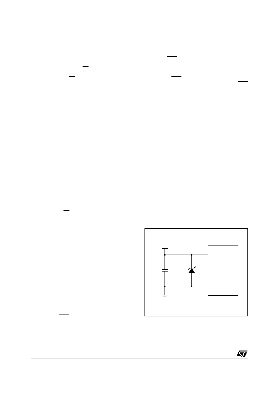
VCC Noise And Negative Going Transients
ICC transients, including those produced by output
switching, can produce voltage fluctuations, re-
sulting in spikes on the VCC bus. These transients
can be reduced if capacitors are used to store en-
ergy which stabilizes the VCC bus. The energy
stored in the bypass capacitors will be released as
low going spikes are generated or energy will be
absorbed when overshoots occur. A ceramic by-
pass capacitor value of 0.1F (as shown in Figure
13) is recommended in order to provide the need-
ed filtering.
In addition to transients that are caused by normal
SRAM operation, power cycling can generate neg-
ative voltage spikes on VCC that drive it to values
below VSS by as much as one volt. These negative
spikes can cause data corruption in the SRAM
while in battery backup mode. To protect from
these voltage spikes, STMicroelectronics recom-
mends connecting a schottky diode from VCC to
VSS (cathode connected to VCC, anode to VSS).
Schottky diode 1N5817 is recommended for
through hole and MBRS120T3 is recommended
for surface mount.
Figure 13. Supply Voltage Protection
AI00622
VCC
0.1
F
DEVICE
VCC
VSS
相關(guān)PDF資料 |
PDF描述 |
|---|---|
| M40SZ100WSH | 5V or 3V NVRAM SUPERVISOR FOR LPSRAM |
| M40SZ100Y | 5V or 3V NVRAM SUPERVISOR FOR LPSRAM |
| M41ST84Y | 5.0 or 3.0V, 512 bit 64 x 8 SERIAL RTC with SUPERVISORY FUNCTIONS |
| M45PE10-VMN6G | 4 Mbit Uniform Sector, Serial Flash Memory |
| M45PE10-VMN6P | 4 Mbit Uniform Sector, Serial Flash Memory |
相關(guān)代理商/技術(shù)參數(shù) |
參數(shù)描述 |
|---|---|
| M40SZ100WMQ6 | 功能描述:監(jiān)控電路 Single Low Pwr SRAM RoHS:否 制造商:STMicroelectronics 監(jiān)測電壓數(shù): 監(jiān)測電壓: 欠電壓閾值: 過電壓閾值: 輸出類型:Active Low, Open Drain 人工復(fù)位:Resettable 監(jiān)視器:No Watchdog 電池備用開關(guān):No Backup 上電復(fù)位延遲(典型值):10 s 電源電壓-最大:5.5 V 最大工作溫度:+ 85 C 安裝風(fēng)格:SMD/SMT 封裝 / 箱體:UDFN-6 封裝:Reel |
| M40SZ100WMQ6E | 功能描述:監(jiān)控電路 Single Low Pwr SRAM RoHS:否 制造商:STMicroelectronics 監(jiān)測電壓數(shù): 監(jiān)測電壓: 欠電壓閾值: 過電壓閾值: 輸出類型:Active Low, Open Drain 人工復(fù)位:Resettable 監(jiān)視器:No Watchdog 電池備用開關(guān):No Backup 上電復(fù)位延遲(典型值):10 s 電源電壓-最大:5.5 V 最大工作溫度:+ 85 C 安裝風(fēng)格:SMD/SMT 封裝 / 箱體:UDFN-6 封裝:Reel |
| M40SZ100WMQ6ETR | 制造商:STMicroelectronics 功能描述:PROCESSOR SUPERVISOR 500UA 16SOIC - Bulk |
| M40SZ100WMQ6F | 功能描述:監(jiān)控電路 Single Low Pwr SRAM RoHS:否 制造商:STMicroelectronics 監(jiān)測電壓數(shù): 監(jiān)測電壓: 欠電壓閾值: 過電壓閾值: 輸出類型:Active Low, Open Drain 人工復(fù)位:Resettable 監(jiān)視器:No Watchdog 電池備用開關(guān):No Backup 上電復(fù)位延遲(典型值):10 s 電源電壓-最大:5.5 V 最大工作溫度:+ 85 C 安裝風(fēng)格:SMD/SMT 封裝 / 箱體:UDFN-6 封裝:Reel |
| M40SZ100WMQ6FTR | 制造商:STMicroelectronics 功能描述:PROCESSOR SUPERVISOR 500UA 16SOIC - Tape and Reel |
發(fā)布緊急采購,3分鐘左右您將得到回復(fù)。