- 您現(xiàn)在的位置:買賣IC網(wǎng) > PDF目錄370849 > M37905M4C (Mitsubishi Electric Corporation) DIODE SCHOTTKY DUAL COMMON-ANODE 25V 200mW 0.32V-vf 200mA-IFM 1mA-IF 2uA-IR SOT-323 3K/REEL PDF資料下載
參數(shù)資料
| 型號: | M37905M4C |
| 廠商: | Mitsubishi Electric Corporation |
| 英文描述: | DIODE SCHOTTKY DUAL COMMON-ANODE 25V 200mW 0.32V-vf 200mA-IFM 1mA-IF 2uA-IR SOT-323 3K/REEL |
| 中文描述: | 16位CMOS微機(jī) |
| 文件頁數(shù): | 83/102頁 |
| 文件大小: | 881K |
| 代理商: | M37905M4C |
第1頁第2頁第3頁第4頁第5頁第6頁第7頁第8頁第9頁第10頁第11頁第12頁第13頁第14頁第15頁第16頁第17頁第18頁第19頁第20頁第21頁第22頁第23頁第24頁第25頁第26頁第27頁第28頁第29頁第30頁第31頁第32頁第33頁第34頁第35頁第36頁第37頁第38頁第39頁第40頁第41頁第42頁第43頁第44頁第45頁第46頁第47頁第48頁第49頁第50頁第51頁第52頁第53頁第54頁第55頁第56頁第57頁第58頁第59頁第60頁第61頁第62頁第63頁第64頁第65頁第66頁第67頁第68頁第69頁第70頁第71頁第72頁第73頁第74頁第75頁第76頁第77頁第78頁第79頁第80頁第81頁第82頁當(dāng)前第83頁第84頁第85頁第86頁第87頁第88頁第89頁第90頁第91頁第92頁第93頁第94頁第95頁第96頁第97頁第98頁第99頁第100頁第101頁第102頁
83
M37905M4C-XXXFP, M37905M4C-XXXSP
M37905M6C-XXXFP, M37905M6C-XXXSP
M37905M8C-XXXFP, M37905M8C-XXXSP
PRELIMINARY
Notice: This is not a final specification.
Some parametric limits are subject to change.
16-BIT CMOS MICROCOMPUTER
MITSUBISHI MICROCOMPUTERS
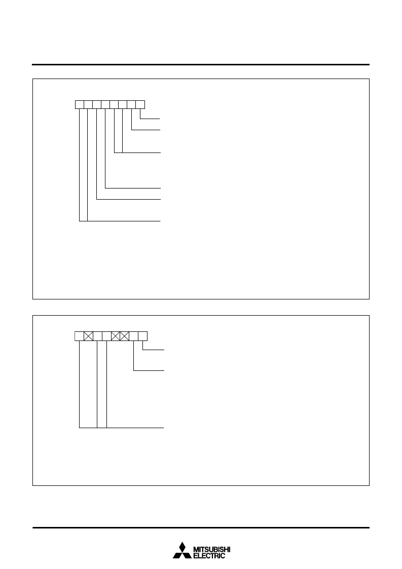
Fig. 95 Bit configuration of particular function select register 0
Fig. 94 Bit configuration of clock control register 0
7
0
6
5
0
4
0
3
2
1
0
Particular function select register 0
External clock input select bit
(Note)
0: Oscillation circuit is active. (The oscillator is connected.)
Watchdog timer is used at stop mode termination.
1: Oscillation circuit is inactive. (The externally-generated clock is input.)
When the system clock select bit =
“
0
”
,
watchdog timer is not used at stop mode termination.
When the system clock select bit =
“
1
”
,
watchdog timer is used at stop mode termination.
Fix this bit to
“
0
”
.
STP instruction invalidity select bit
(Note)
0: STP instruction is valid.
1: STP instruction is invalid.
Note:
Address
62
16
Writing to these bits requires the following procedure:
Write
“
55
16
”
to this register. (The bit status does not change only by this writing.)
Succeedingly, write
“
0
”
or
“
1
”
to each bit.
Also, use the
MOVM (MOVMB)
instruction or
STA (STAB, STAD)
instruction
7
6
5
4
1
3
2
1
0
1
Clock control register 0
Fix this bit to
“
1
”
.
PLL circuit operation enable bit
(Note 1)
0: PLL frequency multiplier is inactive, and pin V
CONT
is invalid (floating state).
1: PLL frequency multiplier is active, and pin V
CONT
is valid.
PLL multiplication ratio select bits
(Note 2)
00: Do not select.
01: Double
10: Triple
11: Quadruple
Fix this bit to
“
1
”
.
System clock select bit
(Note 3)
0: fX
IN
1: f
PLL
Peripheral device
’
s clock select bits 1, 0
See Table 10.
Address
BC
16
Notes 1:
When not using the PLL frequency multiplier, be sure to clear this bit to
“
0
”
.
In the stop mode, the PLL circuit is inactive regardless of this bit
’
s content; at this time, pin
V
CONT
is invalid.
2:
When rewriting this bit, be sure to clear bit 5 to
“
0
”
simultaneously. Also, after this bit is
rewritten, insert a waiting time of 2 ms, and then set bit 5 to
“
1
”
.
3:
When the PLL circuit operation enable bit (bit 1) has been cleared to
“
0
”
, this bit will also be
cleared to
“
0
”
. When bit 1 =
“
0
”
, nothing can be written to this bit. (Fixed to be
“
0
”
.)
相關(guān)PDF資料 |
PDF描述 |
|---|---|
| M37905M4C-XXXFP | 16 BIT CMOS MICROCOMPUTER |
| M37905M4C-XXXSP | 16 BIT CMOS MICROCOMPUTER |
| M37905M6C-XXXFP | DIODE SCHOTTKY DUAL-DUAL SERIES 25V 200mW 0.32V-vf 200mA-IFM 1mA-IF 2uA-IR SOT-363 3K/REEL |
| M37905M6C-XXXSP | DIO, BAT54C, DUAL SHOTTKEY, COMMON CATHODE, SOT23 |
| M37905M8C-XXXFP | 16 BIT CMOS MICROCOMPUTER |
相關(guān)代理商/技術(shù)參數(shù) |
參數(shù)描述 |
|---|---|
| M37905M4C-XXXFP | 制造商:MITSUBISHI 制造商全稱:Mitsubishi Electric Semiconductor 功能描述:16 BIT CMOS MICROCOMPUTER |
| M37905M4C-XXXSP | 制造商:MITSUBISHI 制造商全稱:Mitsubishi Electric Semiconductor 功能描述:16 BIT CMOS MICROCOMPUTER |
| M37905M6C-XXXFP | 制造商:MITSUBISHI 制造商全稱:Mitsubishi Electric Semiconductor 功能描述:16 BIT CMOS MICROCOMPUTER |
| M37905M6C-XXXSP | 制造商:MITSUBISHI 制造商全稱:Mitsubishi Electric Semiconductor 功能描述:16 BIT CMOS MICROCOMPUTER |
| M37905M8C-XXXFP | 制造商:MITSUBISHI 制造商全稱:Mitsubishi Electric Semiconductor 功能描述:16 BIT CMOS MICROCOMPUTER |
發(fā)布緊急采購,3分鐘左右您將得到回復(fù)。