- 您現(xiàn)在的位置:買賣IC網(wǎng) > PDF目錄370849 > M37736EHBXXXGP (Mitsubishi Electric Corporation) PROM VERSION OF M37736MHBXXXGP(MICROCOMPUTERS) PDF資料下載
參數(shù)資料
| 型號: | M37736EHBXXXGP |
| 廠商: | Mitsubishi Electric Corporation |
| 英文描述: | PROM VERSION OF M37736MHBXXXGP(MICROCOMPUTERS) |
| 中文描述: | PROM的版本M37736MHBXXXGP(微型) |
| 文件頁數(shù): | 30/96頁 |
| 文件大?。?/td> | 1328K |
| 代理商: | M37736EHBXXXGP |
第1頁第2頁第3頁第4頁第5頁第6頁第7頁第8頁第9頁第10頁第11頁第12頁第13頁第14頁第15頁第16頁第17頁第18頁第19頁第20頁第21頁第22頁第23頁第24頁第25頁第26頁第27頁第28頁第29頁當(dāng)前第30頁第31頁第32頁第33頁第34頁第35頁第36頁第37頁第38頁第39頁第40頁第41頁第42頁第43頁第44頁第45頁第46頁第47頁第48頁第49頁第50頁第51頁第52頁第53頁第54頁第55頁第56頁第57頁第58頁第59頁第60頁第61頁第62頁第63頁第64頁第65頁第66頁第67頁第68頁第69頁第70頁第71頁第72頁第73頁第74頁第75頁第76頁第77頁第78頁第79頁第80頁第81頁第82頁第83頁第84頁第85頁第86頁第87頁第88頁第89頁第90頁第91頁第92頁第93頁第94頁第95頁第96頁
PRELIMINARY
Notice: This is not a final specification.
Some parametric limits are subject to change.
MITSUBISHI MICROCOMPUTERS
M37736MHBXXXGP
SINGLE-CHIP 16-BIT CMOS MICROCOMPUTER
30
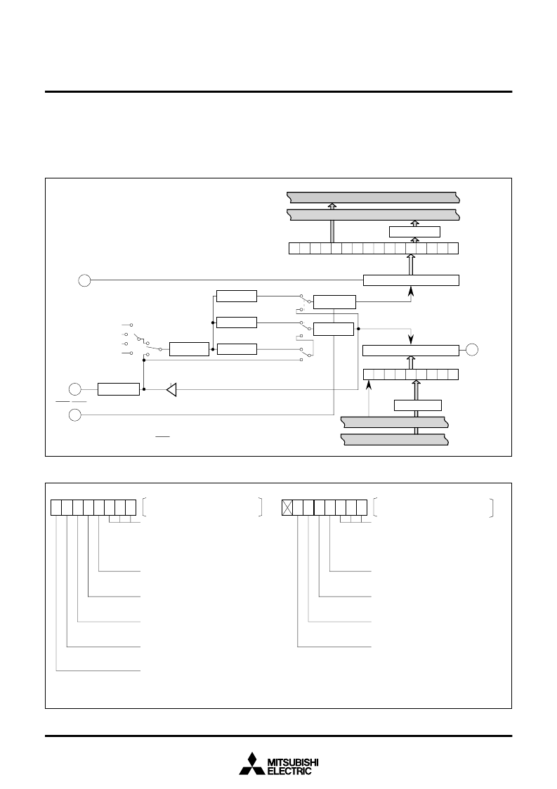
SERIAL I/O PORTS
Three independent serial I/O ports are provided.
Figure 36 shows a block diagram of the serial I/O ports.
Table 5 shows the functional differences of three serial I/O ports
(UART 0, 1, 2).
Bits 0, 1, and 2 of the UARTi (i = 0, 1, 2) transmit/receive mode
register shown in Figure 37 are used to determine whether to use
port P8 or port P10 as a parallel port, a clock synchronous serial I/O
port, or an asynchronous serial I/O port (UART) using start and stop
bits.
Fig. 36 Serial I/O port block diagram
Fig. 37 UARTi transmit/receive mode register bit configuration
UART 0 transmit/receive mode register 30
16
UART 1 transmit/receive mode register 38
16
Serial I/O mode selection bits
0 0 0 : Parallel port
0 0 1 : Clock synchronous
1 0 0 : 7-bit UART
1 0 1 : 8-bit UART
1 1 0 : 9-bit UART
Internal clock/External clock selection bit
0 : Internal clock
1 : External clock
Stop bit length selection bit
0 : 1 stop bit
1 : 2 stop bits
Odd/even parity selection bit
0 : Odd parity
1 : Even parity
Parity enable bit
0 : No parity
1 : With parity
Sleep function selection bit
0 : No sleep
1 : Sleep
Addresses
7
6
5 4
3
2 1
0
Data bus (odd)
Data bus (even)
Bit converter
0
0
0
0
0
0
0
D
7
D
6
D
5
D
4
D
3
D
2
D
1
D
0
D
8
Receive register
Receive
buffer register
UART0 (Addresses 37
16
, 36
16
)
UART1 (Addresses 3F
16
, 3E
16
)
UART2 (Addresses 6B
16
, 6A
16
)
Reccircuit
RxDi
Data bus (even)
D
7
D
6
D
5
D
4
D
3
D
2
D
1
D
0
D
8
Transmisson register
UART0 (Addresses 33
16
, 32
16
)
UART1 (Addresses 3B
16
, 3A
16
)
UART2 (Addresses 67
16
, 66
16
)
Bit converter
(Note)
control circuit
Transmission
buffer register
revePolarity
f
2
f
16
f
64
f
512
CLKi
CTSi/RTSi
1/16 Divider
UART receive
Clock synchronous
UART transmission
1/16 Divider
Clock synchronous
Clock synchronous
(Internal clock)
1/2 Divider
Clock synchronous
(External clock)
1/(n + 1)
Divider
External
Internal
Clock source selection
Bit rate
generator
UART0
(Address 31
16
)
UART1
(Address 39
16
)
UART2
(Address 65
16
)
Receive clock
Transmission clock
Data bus (odd)
TxDi
Clock synchronous
(Internal clock)
(Note)
(Note)
(Note)
Note.
UART2 does not include the bit converter, the polarity
reversing circuit and the
RTS
i
output.
UART 2 transmit/receive mode register 64
16
Address
Serial I/O mode selection bits
0 0 1 : Clock synchronous
1 0 0 : 7-bit UART
1 0 1 : 8-bit UART
1 1 0 : 9-bit UART
Internal clock/External clock selection bit
0 : Internal clock
1 : External clock
Stop bit length selection bit
0 : 1 stop bit
1 : 2 stop bits
Odd/even parity selection bit
0 : Odd parity
1 : Even parity
Parity enable bit
0 : No parity
1 : With parity
6 5
4
3 2
1
0
The switch of A-D conversion interrupt and UART2 transmit/receive
interrupt is performed by bits 0 to 2. When selecting a parallel port, A-D
conversion interrupt is valid. When selecting a clock synchronous serial
I/O port or a UART, UART2 transmit/receive interrupt is valid.
Note.
7
(Note)
相關(guān)PDF資料 |
PDF描述 |
|---|---|
| M37736MHBXXXGP | SINGLE-CHIP 16-BIT CMOS MICROCOMPUTER |
| M37753FFCFP | SINGLE CHIP 16 BIT CMOS MICROCOMPUTER FLASH MEMORY VERSION |
| M37753FFCHP | SINGLE CHIP 16 BIT CMOS MICROCOMPUTER FLASH MEMORY VERSION |
| M37754M8C-XXXGP | SINGLE-CHIP 16BIT CMOS MICROCOMPUTER |
| M37754M8C-XXXHP | SINGLE-CHIP 16BIT CMOS MICROCOMPUTER |
相關(guān)代理商/技術(shù)參數(shù) |
參數(shù)描述 |
|---|---|
| M37736EHL | 制造商:MITSUBISHI 制造商全稱:Mitsubishi Electric Semiconductor 功能描述:PROM VERSION OF M37736MHLXXXHP(MICROCOMPUTERS) |
| M37736EHLXXXHP | 制造商:RENESAS 制造商全稱:Renesas Technology Corp 功能描述:PROM VERSION OF M37736MHLXXXHP |
| M37736M4B | 制造商:MITSUBISHI 制造商全稱:Mitsubishi Electric Semiconductor 功能描述:SINGLE-CHIP 16-BIT CMOS MICROCOMPUTER |
| M37736M4BXXXGP | 制造商:MITSUBISHI 制造商全稱:Mitsubishi Electric Semiconductor 功能描述:SINGLE-CHIP 16-BIT CMOS MICROCOMPUTER |
| M37736M4L | 制造商:MITSUBISHI 制造商全稱:Mitsubishi Electric Semiconductor 功能描述:SINGLE-CHIP 16-BIT CMOS MICROCOMPUTER |
發(fā)布緊急采購,3分鐘左右您將得到回復(fù)。