- 您現(xiàn)在的位置:買(mǎi)賣(mài)IC網(wǎng) > PDF目錄45036 > M37641M8-XXXFP 8-BIT, MROM, 24 MHz, MICROCONTROLLER, PQFP80 PDF資料下載
參數(shù)資料
| 型號(hào): | M37641M8-XXXFP |
| 元件分類: | 微控制器/微處理器 |
| 英文描述: | 8-BIT, MROM, 24 MHz, MICROCONTROLLER, PQFP80 |
| 封裝: | 14 X 20 MM, 0.80 MM PITCH, PLASTIC, QFP-80 |
| 文件頁(yè)數(shù): | 92/136頁(yè) |
| 文件大小: | 1672K |
| 代理商: | M37641M8-XXXFP |
第1頁(yè)第2頁(yè)第3頁(yè)第4頁(yè)第5頁(yè)第6頁(yè)第7頁(yè)第8頁(yè)第9頁(yè)第10頁(yè)第11頁(yè)第12頁(yè)第13頁(yè)第14頁(yè)第15頁(yè)第16頁(yè)第17頁(yè)第18頁(yè)第19頁(yè)第20頁(yè)第21頁(yè)第22頁(yè)第23頁(yè)第24頁(yè)第25頁(yè)第26頁(yè)第27頁(yè)第28頁(yè)第29頁(yè)第30頁(yè)第31頁(yè)第32頁(yè)第33頁(yè)第34頁(yè)第35頁(yè)第36頁(yè)第37頁(yè)第38頁(yè)第39頁(yè)第40頁(yè)第41頁(yè)第42頁(yè)第43頁(yè)第44頁(yè)第45頁(yè)第46頁(yè)第47頁(yè)第48頁(yè)第49頁(yè)第50頁(yè)第51頁(yè)第52頁(yè)第53頁(yè)第54頁(yè)第55頁(yè)第56頁(yè)第57頁(yè)第58頁(yè)第59頁(yè)第60頁(yè)第61頁(yè)第62頁(yè)第63頁(yè)第64頁(yè)第65頁(yè)第66頁(yè)第67頁(yè)第68頁(yè)第69頁(yè)第70頁(yè)第71頁(yè)第72頁(yè)第73頁(yè)第74頁(yè)第75頁(yè)第76頁(yè)第77頁(yè)第78頁(yè)第79頁(yè)第80頁(yè)第81頁(yè)第82頁(yè)第83頁(yè)第84頁(yè)第85頁(yè)第86頁(yè)第87頁(yè)第88頁(yè)第89頁(yè)第90頁(yè)第91頁(yè)當(dāng)前第92頁(yè)第93頁(yè)第94頁(yè)第95頁(yè)第96頁(yè)第97頁(yè)第98頁(yè)第99頁(yè)第100頁(yè)第101頁(yè)第102頁(yè)第103頁(yè)第104頁(yè)第105頁(yè)第106頁(yè)第107頁(yè)第108頁(yè)第109頁(yè)第110頁(yè)第111頁(yè)第112頁(yè)第113頁(yè)第114頁(yè)第115頁(yè)第116頁(yè)第117頁(yè)第118頁(yè)第119頁(yè)第120頁(yè)第121頁(yè)第122頁(yè)第123頁(yè)第124頁(yè)第125頁(yè)第126頁(yè)第127頁(yè)第128頁(yè)第129頁(yè)第130頁(yè)第131頁(yè)第132頁(yè)第133頁(yè)第134頁(yè)第135頁(yè)第136頁(yè)
59
7641 Group
SINGLE-CHIP 8-BIT CMOS MICROCOMPUTER
MITSUBISHI MICROCOMPUTERS
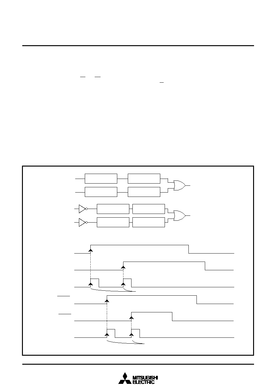
Fig. 54 Interrupt request circuit of data bus buffer
MASTER CPU BUS INTERFACE
The 7641 group internally has a 2-byte bus interface which control
signals from the host CPU side can operate (slave mode).
This bus interface allows the 7641 group to be directly connected
with a R/W type of CPU bus or a RD and WR separated type of
CPU bus. Figure 56 shows the block diagram of master CPU bus
interface function.
The data bus buffer function I/O pins (P52 – P57, P6, P72–P74)
also function as the normal I/O ports. When the Master CPU Bus
Interface Enable bit of Data Bus Buffer Control Register (bit 6 of
address 004A16) is “0”, these pins become the normal I/O ports.
When it is “1”, these pins become the master CPU bus interface
function pins.
Additionally, when using the master CPU bus interface function,
set port P6 to input mode by setting “0016” into its port direction
register (address 001516).
The selection of either the single data bus buffer mode, which
uses 1 byte: data bus buffer 0 only, or the double data bus buffer
mode, which uses 2 bytes: data bus buffer 0 and data bus buffer
1, is performed by the Data Bus Buffer Function Select Bit of Data
Bus Buffer Control Register 1 (bit 7 of address 004E16). Port P72
becomes S1 input pin in the double data bus buffer mode.
When data is written from the host CPU side, an input buffer full
interrupt occurs. When data is read from the host CPU, an output
buffer empty interrupt occurs. The 7641 group shares two input
buffer full interrupt requests and two output buffer empty interrupt
requests as shown in Figure 54, respectively.
The 7641 group can also operate the master CPU bus interface
connecting with the Built-in DMAC. This could transfer a large
amount of data fast.
An input signal level of data bus buffer function input pins can be
selected between a CMOS level and a TTL level. Set it using the
Master CPU Bus Input Level Select Bit of Port Control Register
(address 001016)
.
Input buffer
full flag 0
IBF0
Input buffer
full flag 1
IBF1
Rising edge
detection circuit
One-shot pulse
generating circuit
One-shot pulse
generating circuit
Input buffer full interrupt
request signal IBF
Output buffer
full flag 0
OBF0
Output buffer
full flag 1
OBF1
One-shot pulse
generating circuit
One-shot pulse
generating circuit
Output buffer empty interrupt
request signal OBE
Interrupt request is set at this rising edge
IBF0
IBF1
IBF
OBF0
(
OBE0)
OBF1
(
OBE1)
OBE
OBE0
OBE1
Rising edge
detection circuit
Rising edge
detection circuit
Rising edge
detection circuit
相關(guān)PDF資料 |
PDF描述 |
|---|---|
| M37643M8-XXXFP | 8-BIT, MROM, 12 MHz, MICROCONTROLLER, PQFP80 |
| M37643F8HP | 8-BIT, FLASH, 12 MHz, MICROCONTROLLER, PQFP80 |
| M37643M8-XXXHP | 8-BIT, MROM, 12 MHz, MICROCONTROLLER, PQFP80 |
| M37700M2-XXXFP | 16-BIT, MROM, 8 MHz, MICROCONTROLLER, PQFP80 |
| M37701M2-001SP | 16-BIT, MROM, 8 MHz, MICROCONTROLLER, PDIP64 |
相關(guān)代理商/技術(shù)參數(shù) |
參數(shù)描述 |
|---|---|
| M37641M8-XXXHP | 制造商:MITSUBISHI 制造商全稱:Mitsubishi Electric Semiconductor 功能描述:SINGLE-CHIP 8-BIT CMOS MICROCOMPUTER |
| M376420RS | 制造商:OKI 功能描述:3764-20 NOTES |
| M3764-20RS | 制造商:OKI 功能描述:3764-20 NOTES 制造商: 功能描述:Dynamic RAM, Page Mode, 64K x 1, 16 Pin, Plastic, DIP 制造商:OK International 功能描述:Dynamic RAM, Page Mode, 64K x 1, 16 Pin, Plastic, DIP |
| M3-7643A-S | 制造商:Harris Corporation 功能描述: |
| M37643F8E8-XXXFP | 制造商:RENESAS 制造商全稱:Renesas Technology Corp 功能描述:SINGLE-CHIP 8-BIT CMOS MICROCOMPUTER |
發(fā)布緊急采購(gòu),3分鐘左右您將得到回復(fù)。