- 您現在的位置:買賣IC網 > PDF目錄385508 > M37225M8 (Mitsubishi Electric Corporation) SINGLE-CHIP 8-BIT CMOS MICROCOMPUTER for VOLTAGE SYNTHESIZER with ON-SCREEN DISPLAY CONTROLLER PDF資料下載
參數資料
| 型號: | M37225M8 |
| 廠商: | Mitsubishi Electric Corporation |
| 英文描述: | SINGLE-CHIP 8-BIT CMOS MICROCOMPUTER for VOLTAGE SYNTHESIZER with ON-SCREEN DISPLAY CONTROLLER |
| 中文描述: | 單芯片8位CMOS微機電壓合成與屏幕顯示控制器 |
| 文件頁數: | 59/133頁 |
| 文件大小: | 1610K |
| 代理商: | M37225M8 |
第1頁第2頁第3頁第4頁第5頁第6頁第7頁第8頁第9頁第10頁第11頁第12頁第13頁第14頁第15頁第16頁第17頁第18頁第19頁第20頁第21頁第22頁第23頁第24頁第25頁第26頁第27頁第28頁第29頁第30頁第31頁第32頁第33頁第34頁第35頁第36頁第37頁第38頁第39頁第40頁第41頁第42頁第43頁第44頁第45頁第46頁第47頁第48頁第49頁第50頁第51頁第52頁第53頁第54頁第55頁第56頁第57頁第58頁當前第59頁第60頁第61頁第62頁第63頁第64頁第65頁第66頁第67頁第68頁第69頁第70頁第71頁第72頁第73頁第74頁第75頁第76頁第77頁第78頁第79頁第80頁第81頁第82頁第83頁第84頁第85頁第86頁第87頁第88頁第89頁第90頁第91頁第92頁第93頁第94頁第95頁第96頁第97頁第98頁第99頁第100頁第101頁第102頁第103頁第104頁第105頁第106頁第107頁第108頁第109頁第110頁第111頁第112頁第113頁第114頁第115頁第116頁第117頁第118頁第119頁第120頁第121頁第122頁第123頁第124頁第125頁第126頁第127頁第128頁第129頁第130頁第131頁第132頁第133頁
59
SINGLE-CHIP 8-BIT CMOS MICROCOMPUTER for VOLTAGE SYNTHESIZER
with ON-SCREEN DISPLAY CONTROLLER
M37225M6–XXXSP, M37225M8–XXXSP
M37225ECSP
MITSUBISHI MICROCOMPUTERS
Rev. 1.0
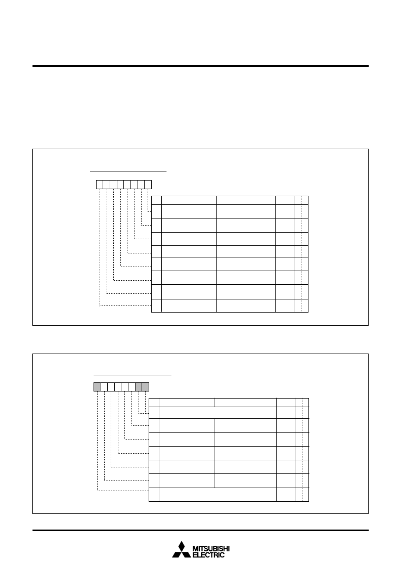
(3) OSD input/output pin control
The OSD output pins R, G, B, OUT1 and OUT2 can also function as
ports P5
2
, P5
3
, P5
4
, P5
5
, P1
0
respectively. Switch either OSD out-
put function or port function by the OSD port control register (ad-
dress 00CB
16
).
The input polarity of the H
SYNC
, V
SYNC
and output polarity of signals
R, G, B, OUT1 and OUT2 can be specified with the OSD I/O polarity
register (address 00EB
16
). Set a bit to “0” to specify positive polarity;
Fig. 8.10.6 OSD I/O Polarity Register
7 b
6 b
5 b
4 b
3 b
2 b
1 b
0
O
S
D
I
/
O
p
o
l
a
r
i
t
y
r
e
g
i
s
t
e
r
(
O
P
C
)
[
A
d
d
r
e
s
s
0
0
E
B
1
6
]
B
N
a
m
e
F
u
n
c
t
i
o
n
s
A
f
t
e
r
r
e
R
W
O
S
D
I
/
O
P
o
l
a
r
i
t
y
R
e
g
i
s
t
e
r
0
H
S
s
w
Y
i
t
N
c
C
h
i
b
n
p
i
t
u
(
t
p
P
o
C
l
a
0
r
)
i
t
y
O
0
1
1
1
1
:
P
N
o
e
s
g
i
a
t
i
v
t
e
v
e
p
o
p
l
o
a
l
r
a
i
r
t
y
i
t
y
i
n
i
p
n
u
p
t
u
:
i
t
0
1
0
:
P
N
o
e
s
g
i
a
t
i
v
t
e
v
e
p
o
p
l
o
a
l
r
a
i
r
t
y
i
t
y
i
n
i
p
n
u
p
t
u
:
i
t
0
2
R
b
U
s
w
/
G
t
/
O
B
o
C
u
2
t
p
)
u
t
p
o
l
a
r
i
t
y
s
w
i
t
c
h
i
(
P
0
:
P
N
o
e
s
g
i
a
t
i
v
t
e
v
e
p
o
p
l
o
a
l
r
a
i
r
t
y
i
t
y
o
u
o
t
u
p
t
u
p
t
u
:
i
t
0
3
0
V
S
s
w
Y
i
N
t
c
C
h
i
n
b
p
i
t
u
(
t
O
p
P
o
C
l
a
1
r
i
t
y
)
R
W
R
W
R
W
R
W
4
O
s
a
b
i
a
(
O
a
(
O
U
w
T
t
c
2
h
o
b
u
i
t
p
(
u
O
t
P
p
C
o
l
a
)
r
i
t
y
i
t
4
0
1
1
1
:
P
N
o
e
s
g
i
a
t
i
v
t
e
v
e
p
o
p
l
o
a
l
r
a
i
r
t
y
i
t
y
o
u
o
t
u
p
t
u
p
t
u
:
i
t
0
5
R
s
(
t
O
e
r
c
C
o
5
l
)
o
r
R
c
o
n
t
r
o
l
t
P
0
:
N
O
o
u
t
o
p
u
u
t
t
p
u
t
:
0
6
R
s
P
t
C
e
r
6
c
)
o
l
o
r
G
c
o
n
t
r
o
l
b
i
t
0
7
R
s
P
t
C
e
r
7
c
)
o
l
o
r
B
c
o
n
t
r
o
l
b
i
t
0
1
:
N
O
o
u
t
o
p
u
u
t
t
p
u
t
:
0
R
W
R
W
R
W
R W
O
T
t
c
1
h
o
b
u
i
t
p
(
u
O
t
P
p
C
o
l
a
)
r
i
t
y
i
t
3
0
:
P
N
o
e
s
g
i
a
t
i
v
t
e
v
e
p
o
p
l
o
a
l
r
a
i
r
t
y
i
t
y
o
u
o
t
u
p
t
u
p
t
u
:
i
t
0
:
N
O
o
u
t
o
p
u
u
t
t
p
u
t
:
set it to “1” to specify negative polarity.
Figure 8.10.6 shows the OSD I/O polarity register and Figure 8.10.7
shows the OSD port control register.
Fig. 8.10.7 OSD Port Control Register
7 b
0
6 b
5 b
4 b
3 b
2 b
1 b
0
0
0
O
S
D
p
o
r
t
c
o
n
t
r
o
l
r
e
g
i
s
t
e
r
(
P
F
)
[
A
d
d
r
e
s
s
0
0
C
B
1
6
]
b
N
a
m
e
F
u
n
c
t
i
o
n
s
A
f
t
e
r
r
e
s
e
t
R W
O
S
D
P
o
r
t
C
o
n
t
r
o
l
R
e
g
i
s
t
e
r
0
,
1
0
R W
F
i
x
t
h
e
s
e
b
i
t
s
t
o
“
0
”
2
0
1
1
1
1
1
:
R
P
o
s
r
i
t
g
n
P
a
5
2
l
o
o
u
u
t
t
p
p
u
u
t
t
:
0
R W
3
P
s
o
s
e
o
s
e
o
s
e
i
o
e
r
l
e
t
c
P
t
5
3
i
o
o
n
u
t
t
p
(
u
P
t
s
3
i
g
S
n
E
a
L
l
)
b
i
5
0
:
G
P
o
s
r
i
t
g
n
P
a
5
3
l
o
o
u
u
t
t
p
p
u
u
t
t
:
0
R W
4
P
r
l
e
t
c
P
t
5
4
i
o
o
n
u
t
t
p
(
u
P
t
s
4
i
g
S
n
E
a
L
l
)
b
i
5
0
:
B
P
o
s
i
t
g
n
P
a
5
4
l
o
o
u
u
t
p
t
p
u
u
t
:
r
t
0
R W
5
P
r
l
e
t
c
P
t
5
5
i
o
o
n
u
t
t
p
(
u
P
t
s
5
i
g
S
n
E
a
L
l
)
b
i
5
0
:
O
P
U
o
T
r
t
1
P
5
5
s
i
g
n
o
a
u
l
p
o
u
u
t
t
p
u
t
:
t
0
R W
6
P
r
l
e
t
c
P
t
1
0
i
o
o
n
u
t
t
p
(
u
O
t
U
s
i
T
g
n
2
a
S
l
b
i
E
L
)
0
:
P
O
o
U
r
t
T
P
2
1
0
o
s
t
i
g
u
n
t
a
l
o
u
t
p
u
t
:
u
p
0
R W
P
s
o
e
r
l
e
t
c
P
t
5
2
i
o
o
n
u
t
t
p
(
u
P
t
s
2
i
g
S
n
E
a
L
l
)
b
i
5
7
0
R W
F
x
t
h
i
s
b
i
t
t
o
“
0
”
相關PDF資料 |
PDF描述 |
|---|---|
| M37702M4AXXXFP | SINGLE-CHIP 16-BIT CMOS MICROCOMPUTER |
| M37702M4BXXXFP | SINGLE-CHIP 16-BIT CMOS MICROCOMPUTER |
| M37702S4AFP | SINGLE-CHIP 16-BIT CMOS MICROCOMPUTER |
| M37702S4BFP | SINGLE-CHIP 16-BIT CMOS MICROCOMPUTER |
| M3819 | 8-Bit Single Chip Microcomputer(8位單片微控制器) |
相關代理商/技術參數 |
參數描述 |
|---|---|
| M37225MA | 制造商:RENESAS 制造商全稱:Renesas Technology Corp 功能描述:SNGLE-CHIP 8-BIT CMOS MICROCOMPUTER for VOLTAGE SYNTHESIZER with ON-SCREEN DISPLAY CONTROLLER |
| M372429100 | 制造商:ITW Switches 功能描述:IN-RUSH |
| M372429200 | 制造商:ITW Switches 功能描述:IN-RUSH |
| M372499100 | 制造商:ITW Switches 功能描述:IN-RUSH |
| M372499200 | 制造商:ITW Switches 功能描述:HIGH IN-RUSH MINI ROCKER |
發(fā)布緊急采購,3分鐘左右您將得到回復。