- 您現(xiàn)在的位置:買賣IC網(wǎng) > PDF目錄45029 > M37161MF-XXXSP 8-BIT, MROM, 8 MHz, MICROCONTROLLER, PDIP42 PDF資料下載
參數(shù)資料
| 型號: | M37161MF-XXXSP |
| 元件分類: | 微控制器/微處理器 |
| 英文描述: | 8-BIT, MROM, 8 MHz, MICROCONTROLLER, PDIP42 |
| 封裝: | 0.600 INCH, 1.78 MM PITCH, PLASTIC, SDIP-42 |
| 文件頁數(shù): | 74/129頁 |
| 文件大?。?/td> | 1092K |
| 代理商: | M37161MF-XXXSP |
第1頁第2頁第3頁第4頁第5頁第6頁第7頁第8頁第9頁第10頁第11頁第12頁第13頁第14頁第15頁第16頁第17頁第18頁第19頁第20頁第21頁第22頁第23頁第24頁第25頁第26頁第27頁第28頁第29頁第30頁第31頁第32頁第33頁第34頁第35頁第36頁第37頁第38頁第39頁第40頁第41頁第42頁第43頁第44頁第45頁第46頁第47頁第48頁第49頁第50頁第51頁第52頁第53頁第54頁第55頁第56頁第57頁第58頁第59頁第60頁第61頁第62頁第63頁第64頁第65頁第66頁第67頁第68頁第69頁第70頁第71頁第72頁第73頁當(dāng)前第74頁第75頁第76頁第77頁第78頁第79頁第80頁第81頁第82頁第83頁第84頁第85頁第86頁第87頁第88頁第89頁第90頁第91頁第92頁第93頁第94頁第95頁第96頁第97頁第98頁第99頁第100頁第101頁第102頁第103頁第104頁第105頁第106頁第107頁第108頁第109頁第110頁第111頁第112頁第113頁第114頁第115頁第116頁第117頁第118頁第119頁第120頁第121頁第122頁第123頁第124頁第125頁第126頁第127頁第128頁第129頁
Rev.1.00
2003.11.25
page 49 of 128
M37161M8/MA/MF-XXXSP/FP,M37161EFSP/FP
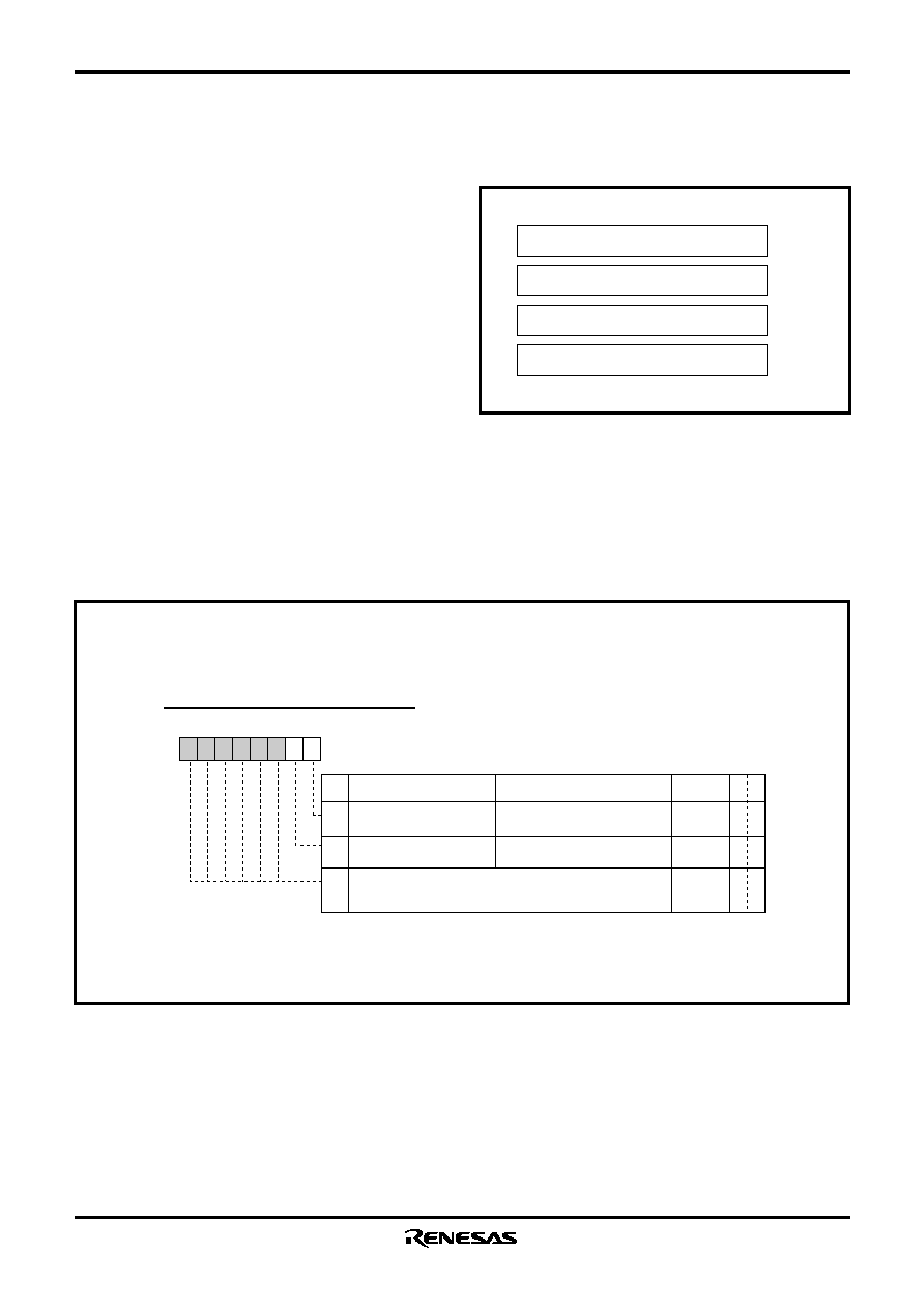
Fig. 8.9.2 ROM Correction Enable Register
Fig. 8.9.1 ROM Correction Address Registers
8.9 ROM CORRECTION FUNCTION
This can correct program data in the ROM. Up to 2 addresses can be
corrected; a program for correction is stored in the ROM correction
vector in the RAM as the top address. There are 2 vectors for ROM
correction :
Vector 1 : address 030016
Vector 2 : address 032016
Set the address of the ROM data to be corrected into the ROM cor-
rection address register. When the value of the counter matches the
ROM data address in the top address of the ROM correction vector,
the main program branches to the correction program stored in the
ROM memory. To return from the correction program to the main
program, the op code and operand of the JMP instruction (total of 3
bytes) are necessary at the end of the correction program.
The ROM correction function is controlled by the ROM correction
enable register.
Notes 1: Specify the first address (op code address) of each
instruction as the ROM correction address.
2: Use the JMP instruction (total of 3 bytes) to return from
the correction program to the main program.
3: Do not set the same ROM correction address to both vectors 1
and 2.
020A16
ROM correction address 1 (high-order)
020B16
ROM correction address 1 (low-order)
020C16
ROM correction address 2 (high-order)
020D16
ROM correction address 2 (low-order)
b7 b6 b5 b4 b3 b2 b1 b0
ROM correction enable register (RCR) [Address 020E 16]
B
After reset
RW
ROM Correction Enable Register
0
Vector 1 enable bit (RC0)
Name
Functions
0: Disabled
1: Enabled
1
Vector 2 enable bit (RC1)
0: Disabled
1: Enabled
2
to
7
Nothing is assigned. These bits are write disable bits. When
these bits are read out, the values are “0.”
0
RW
R —
相關(guān)PDF資料 |
PDF描述 |
|---|---|
| M37161EFSP | 8-BIT, OTPROM, 8 MHz, MICROCONTROLLER, PDIP42 |
| M37161MA-XXXSP | 8-BIT, MROM, 8 MHz, MICROCONTROLLER, PDIP42 |
| M37161M8-XXXSP | 8-BIT, MROM, 8 MHz, MICROCONTROLLER, PDIP42 |
| M37202E3SP | 8-BIT, OTPROM, 4 MHz, MICROCONTROLLER, PDIP64 |
| M37207EFFP | 8-BIT, OTPROM, 8.1 MHz, MICROCONTROLLER, PQFP80 |
相關(guān)代理商/技術(shù)參數(shù) |
參數(shù)描述 |
|---|---|
| M3720 | 制造商:未知廠家 制造商全稱:未知廠家 功能描述:1 KEY 1 SOUND |
| M3720-1 | 制造商:未知廠家 制造商全稱:未知廠家 功能描述:1 KEY 1 SOUND |
| M3720-10 | 制造商:未知廠家 制造商全稱:未知廠家 功能描述:1 KEY 1 SOUND |
| M3720-2 | 制造商:未知廠家 制造商全稱:未知廠家 功能描述:1 KEY 1 SOUND |
| M3720-3 | 制造商:未知廠家 制造商全稱:未知廠家 功能描述:1 KEY 1 SOUND |
發(fā)布緊急采購,3分鐘左右您將得到回復(fù)。