- 您現(xiàn)在的位置:買賣IC網(wǎng) > PDF目錄45029 > M37150M8-XXXFP 8-BIT, MROM, 8.95 MHz, MICROCONTROLLER, PDSO42 PDF資料下載
參數(shù)資料
| 型號(hào): | M37150M8-XXXFP |
| 元件分類: | 微控制器/微處理器 |
| 英文描述: | 8-BIT, MROM, 8.95 MHz, MICROCONTROLLER, PDSO42 |
| 封裝: | 0.450 INCH, 0.80 MM PITCH, PLASTIC, SSOP-42 |
| 文件頁數(shù): | 80/142頁 |
| 文件大?。?/td> | 1712K |
| 代理商: | M37150M8-XXXFP |
第1頁第2頁第3頁第4頁第5頁第6頁第7頁第8頁第9頁第10頁第11頁第12頁第13頁第14頁第15頁第16頁第17頁第18頁第19頁第20頁第21頁第22頁第23頁第24頁第25頁第26頁第27頁第28頁第29頁第30頁第31頁第32頁第33頁第34頁第35頁第36頁第37頁第38頁第39頁第40頁第41頁第42頁第43頁第44頁第45頁第46頁第47頁第48頁第49頁第50頁第51頁第52頁第53頁第54頁第55頁第56頁第57頁第58頁第59頁第60頁第61頁第62頁第63頁第64頁第65頁第66頁第67頁第68頁第69頁第70頁第71頁第72頁第73頁第74頁第75頁第76頁第77頁第78頁第79頁當(dāng)前第80頁第81頁第82頁第83頁第84頁第85頁第86頁第87頁第88頁第89頁第90頁第91頁第92頁第93頁第94頁第95頁第96頁第97頁第98頁第99頁第100頁第101頁第102頁第103頁第104頁第105頁第106頁第107頁第108頁第109頁第110頁第111頁第112頁第113頁第114頁第115頁第116頁第117頁第118頁第119頁第120頁第121頁第122頁第123頁第124頁第125頁第126頁第127頁第128頁第129頁第130頁第131頁第132頁第133頁第134頁第135頁第136頁第137頁第138頁第139頁第140頁第141頁第142頁
SINGLE-CHIP 8-BIT CMOS MICROCOMPUTER with CLOSED CAPTION DECODER
and ON-SCREEN DISPLAY CONTROLLER
MITSUBISHI MICROCOMPUTERS
M37150M6/M8/MA/MC/MF-XXXFP, M37150EFFP
41
Rev. 1.0
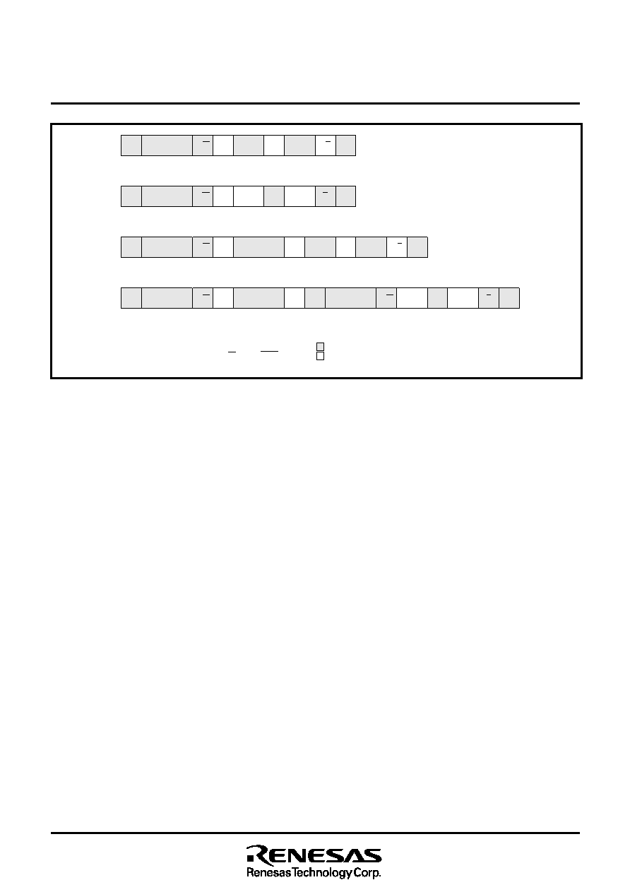
Fig. 8.6.13 Address Data Communication Format
SSlave address
A
DataA
DataA/A
P
R/W
7 bits
“0”
1 to 8 bits
SSlave address
A
Data
AData
A
P
7 bits
“1”
1 to 8 bits
(1) A master-transmitter transmits data to a slave-receiver
S
Slave address
1st 7 bits
A
Data
7 bits
“0”
8 bits
1 to 8 bits
(2) A master-receiver receives data from a slave-transmitter
Slave address
2nd byte
A
DataA/A
P
1 to 8 bits
S
Slave address
1st 7 bits
A
7 bits
“0”
8 bits
7 bits
(3) A master-transmitter transmits data to a slave-receiver with a 10-bit address
Slave address
2nd byte
Data
1 to 8 bits
Sr
Slave address
1st 7 bits
A
Data
A
P
1 to 8 bits
“1”
(4) A master-receiver receives data from a slave-transmitter with a 10-bit address
S: START conditionP : STOP condition
A: ACK bitR/W : Read/Write bit
Sr: Restart condition
From master to slave
From slave to master
R/W
8.6.12 Precautions when using multi-master
I2C-BUS interface
(1) Read-modify-write instruction
Precautions for executing the read-modify-write instructions, such
as SEB, and CLB, is for each register of the multi-master I2C-BUS
interface are described below.
I2C data shift register (S0)
When executing the read-modify-write instruction for this register
during transfer, data may become an arbitrary value.
I2C address register (S0D)
When the read-modify-write instruction is executed for this register
at detection of the STOP condition, data may become an arbitrary
______
value. Because hardware changes the read/write bit (RBW) at the
above timing.
I2C status register (S1)
Do not execute the read-modify-write instruction for this register
because all bits of this register are changed by hardware.
I2C control register (S1D)
When the read-modify-write instruction is executed for this register
at detection of the START condition or at completion of the byte
transfer, data may become an arbitrary value because hardware
changes the bit counter (BC0–BC2) at the above timing.
I2C clock control register (S2)
The read-modify-write instruction can be executed for this register.
(2) START condition generating procedure us-
ing multi-master
Procedure example (The necessary conditions for the procedure
are described in to below).
LDA
—
(Take out slave address value)
SEI
(Interrupt disabled)
BBS 5,S1,BUSBUSY
(BB flag confirmation and branch pro
cess)
BUSFREE:
STA S0
(Write slave address value)
LDM #$F0, S1
(Trigger START condition generation)
CLI
(Interrupt enabled)
BUSBUSY:
CLI
(Interrupt enabled)
Use “STA,” “STX” or “STY” of the zero page addressing instruc-
tion for writing the slave address value to the I2C data shift register.
Use “LDM” instruction for setting trigger of START condition gen-
eration.
Write the slave address value of and set trigger of START con-
dition generation as in continuously, as shown in the procedure
example.
Disable interrupts during the following three process steps:
BB flag confirmation
Write slave address value
Trigger of START condition generation
When the condition of the BB flag is bus busy, enable interrupts
immediately.
相關(guān)PDF資料 |
PDF描述 |
|---|---|
| M37150MF-XXXFP | 8-BIT, MROM, 8.95 MHz, MICROCONTROLLER, PDSO42 |
| M37150MC-XXXFP | 8-BIT, MROM, 8.95 MHz, MICROCONTROLLER, PDSO42 |
| M37151MC-XXXFP | 8-BIT, MROM, 8.1 MHz, MICROCONTROLLER, PDSO42 |
| M37151MF-XXXFP | 8-BIT, MROM, 8.1 MHz, MICROCONTROLLER, PDSO42 |
| M37151M6-XXXFP | 8-BIT, MROM, 8.1 MHz, MICROCONTROLLER, PDSO42 |
相關(guān)代理商/技術(shù)參數(shù) |
參數(shù)描述 |
|---|---|
| M37150MA | 制造商:RENESAS 制造商全稱:Renesas Technology Corp 功能描述:SNGLE-CHIP 8-BIT CMOS MICROCOMPUTER |
| M37150MA-XXXFP | 制造商:RENESAS 制造商全稱:Renesas Technology Corp 功能描述:SNGLE-CHIP 8-BIT CMOS MICROCOMPUTER |
| M37150MC | 制造商:RENESAS 制造商全稱:Renesas Technology Corp 功能描述:SNGLE-CHIP 8-BIT CMOS MICROCOMPUTER |
| M37150MC-XXXFP | 制造商:RENESAS 制造商全稱:Renesas Technology Corp 功能描述:SNGLE-CHIP 8-BIT CMOS MICROCOMPUTER |
| M37150MF | 制造商:RENESAS 制造商全稱:Renesas Technology Corp 功能描述:SNGLE-CHIP 8-BIT CMOS MICROCOMPUTER |
發(fā)布緊急采購,3分鐘左右您將得到回復(fù)。