- 您現在的位置:買賣IC網 > PDF目錄370837 > M30805MG-XXXGP (Mitsubishi Electric Corporation) SINGLE-CHIP 16-BIT CMOS MICROCOMPUTER PDF資料下載
參數資料
| 型號: | M30805MG-XXXGP |
| 廠商: | Mitsubishi Electric Corporation |
| 英文描述: | SINGLE-CHIP 16-BIT CMOS MICROCOMPUTER |
| 中文描述: | 單片16位CMOS微機 |
| 文件頁數: | 147/315頁 |
| 文件大?。?/td> | 4610K |
| 代理商: | M30805MG-XXXGP |
第1頁第2頁第3頁第4頁第5頁第6頁第7頁第8頁第9頁第10頁第11頁第12頁第13頁第14頁第15頁第16頁第17頁第18頁第19頁第20頁第21頁第22頁第23頁第24頁第25頁第26頁第27頁第28頁第29頁第30頁第31頁第32頁第33頁第34頁第35頁第36頁第37頁第38頁第39頁第40頁第41頁第42頁第43頁第44頁第45頁第46頁第47頁第48頁第49頁第50頁第51頁第52頁第53頁第54頁第55頁第56頁第57頁第58頁第59頁第60頁第61頁第62頁第63頁第64頁第65頁第66頁第67頁第68頁第69頁第70頁第71頁第72頁第73頁第74頁第75頁第76頁第77頁第78頁第79頁第80頁第81頁第82頁第83頁第84頁第85頁第86頁第87頁第88頁第89頁第90頁第91頁第92頁第93頁第94頁第95頁第96頁第97頁第98頁第99頁第100頁第101頁第102頁第103頁第104頁第105頁第106頁第107頁第108頁第109頁第110頁第111頁第112頁第113頁第114頁第115頁第116頁第117頁第118頁第119頁第120頁第121頁第122頁第123頁第124頁第125頁第126頁第127頁第128頁第129頁第130頁第131頁第132頁第133頁第134頁第135頁第136頁第137頁第138頁第139頁第140頁第141頁第142頁第143頁第144頁第145頁第146頁當前第147頁第148頁第149頁第150頁第151頁第152頁第153頁第154頁第155頁第156頁第157頁第158頁第159頁第160頁第161頁第162頁第163頁第164頁第165頁第166頁第167頁第168頁第169頁第170頁第171頁第172頁第173頁第174頁第175頁第176頁第177頁第178頁第179頁第180頁第181頁第182頁第183頁第184頁第185頁第186頁第187頁第188頁第189頁第190頁第191頁第192頁第193頁第194頁第195頁第196頁第197頁第198頁第199頁第200頁第201頁第202頁第203頁第204頁第205頁第206頁第207頁第208頁第209頁第210頁第211頁第212頁第213頁第214頁第215頁第216頁第217頁第218頁第219頁第220頁第221頁第222頁第223頁第224頁第225頁第226頁第227頁第228頁第229頁第230頁第231頁第232頁第233頁第234頁第235頁第236頁第237頁第238頁第239頁第240頁第241頁第242頁第243頁第244頁第245頁第246頁第247頁第248頁第249頁第250頁第251頁第252頁第253頁第254頁第255頁第256頁第257頁第258頁第259頁第260頁第261頁第262頁第263頁第264頁第265頁第266頁第267頁第268頁第269頁第270頁第271頁第272頁第273頁第274頁第275頁第276頁第277頁第278頁第279頁第280頁第281頁第282頁第283頁第284頁第285頁第286頁第287頁第288頁第289頁第290頁第291頁第292頁第293頁第294頁第295頁第296頁第297頁第298頁第299頁第300頁第301頁第302頁第303頁第304頁第305頁第306頁第307頁第308頁第309頁第310頁第311頁第312頁第313頁第314頁第315頁
Clock asynchronous serial I/O (UART) mode
deveopmen
Preliminary Specifications REV.B
Specifications in this manual are tentative and subject to change.
Mitsubishi microcomputers
M16C/80 (144-pin version) group
SINGLE-CHIP 16-BIT CMOS MICROCOMPUTER
147
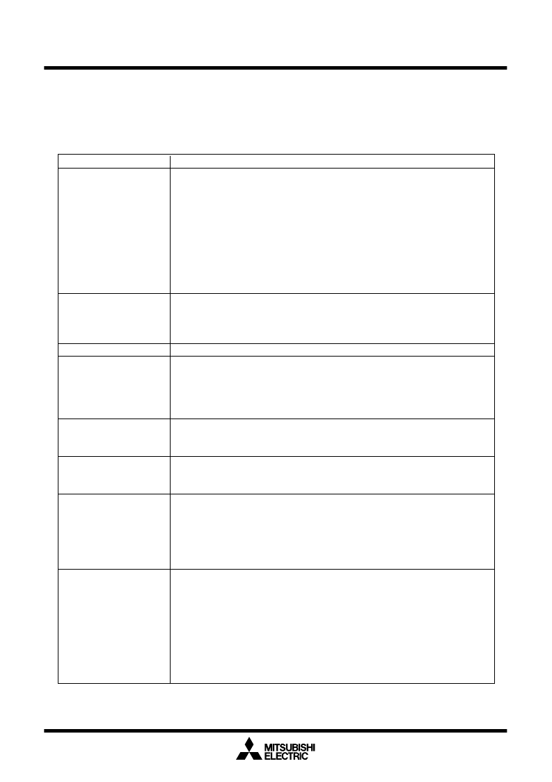
Item
Specification
Transfer data format
Transfer data 8-bit UART mode (bit 2 to 0 of addresses 0338
16
, 0328
16
, 02F8
16
= “101
2
”)
One stop bit (bit 4 of addresses 0338
16
, 0328
16
, 02F8
16
= “0”)
With the direct format chosen
Set parity to “even” (bit 5 and 6 of addresses 0338
16
, 0328
16
, 02F8
16
= “1” and “1” respectively)
Set data logic to “direct” (bit 6 of address 033D
16
= “0”).
Set transfer format to LSB (bit 7 of address 033C
16
= “0”).
With the inverse format chosen
Set parity to “odd” (bit 5 and 6 of addresses 0338
16
, 0328
16
, 02F8
16
= “0” and “1” respectively)
Set data logic to “inverse” (bit 6 of address 033D
16
= “1”)
Set transfer format to MSB (bit 7 of address 033C
16
= “1”)
With the internal clock chosen (bit 3 of
addresses 0338
16
, 0328
16
, 02F8
16
= “0”)
: fi / 16 (n + 1)
(Note 1) : fi=f
1
, f
8
, f
32
With an external clock chosen (bit 3 of
addresses 0338
16
, 0328
16
, 02F8
16
= “1”)
: f
EXT
/ 16 (n+1)
(Note 1) (Note 2)
Disable the CTS and RTS function (bit 4 of address 033C
16
, 032C
16
, 02FC
16
= “1”)
The sleep mode select function is not available for UART2
Set transmission interrupt factor to “transmission completed” (bit 4 of address 033D
16
,
032D
16
, 02FD
16
= “1”)
Set N-channel open drain output to TxD and RxD pins in UART3 and 4 (bit 5 of
address 032C
16
, 02FC
16
= “1”)
To start transmission, the following requirements must be met:
- Transmit enable bit (bit 0 of address 033D
16
, 032D
16
, 02FD
16
) = “1”
- Transmit buffer empty flag (bit 1 of address 033D
16
, 032D
16
, 02FD
16
) = “0”
To start reception, the following requirements must be met:
- Reception enable bit (bit 2 of address 033D
16
, 032D
16
, 02FD
16
) = “1”
- Detection of a start bit
When transmitting
When data transmission from the UART2 to UART4 transfer register is completed (bit
4 of address 033D
16
, 032D
16
, 02FD
16
= “1”)
When receiving
When data transfer from the UART2 to UART4 receive register to the UART2 to
UART4 receive buffer register is completed
Overrun error (see the specifications of clock-asynchronous serial I/O) (Note 3)
Framing error (see the specifications of clock-asynchronous serial I/O)
Parity error (see the specifications of clock-asynchronous serial I/O)
- On the reception side, an “L” level is output from the TxD
i
pin by use of the parity
error signal output function (bit 7 of address 033D
16
, 032D
16
, 02FD
16
= “1”) when a
parity error is detected
- On the transmission side, a parity error is detected by the level of input to the RxD
i
pin when a transmission interrupt occurs
The error sum flag (see the specifications of clock-asynchronous serial I/O)
Note 1: ‘n’ denotes the value 00
16
to FF
16
that is set to the UARTi bit rate generator.
Note 2: f
EXT
is input from the CLKi pin.
Note 3: If an overrun error occurs, the UARTi receive buffer will have the next data written in. Note also
UARTi receive interrupt request bit is not set to “1”.
Transfer clock
Transmission / reception control
Other settings
Transmission start condition
Reception start condition
Error detection
(3) Clock-asynchronous serial I/O mode (compliant with the SIM interface)
The SIM interface is used for connecting the microcomputer with a memory card I/C or the like; adding some
extra settings in UART2 to UART4 clock-asynchronous serial I/O mode allows the user to effect this function.
Table 1.19.1 shows the specifications of clock-asynchronous serial I/O mode (compliant with the SIM interface).
Interrupt request
generation timing
that the
Table 1.19.1. Specifications of clock-asynchronous serial I/O mode (compliant with the SIM interface)
相關PDF資料 |
PDF描述 |
|---|---|
| M30805SGP | SINGLE-CHIP 16-BIT CMOS MICROCOMPUTER |
| M30803FGFP | SINGLE-CHIP 16-BIT CMOS MICROCOMPUTER |
| M30803FGGP | SINGLE-CHIP 16-BIT CMOS MICROCOMPUTER |
| M30803MC-XXXFP | SINGLE-CHIP 16-BIT CMOS MICROCOMPUTER |
| M30803MC-XXXGP | SINGLE-CHIP 16-BIT CMOS MICROCOMPUTER |
相關代理商/技術參數 |
參數描述 |
|---|---|
| M30805SGP | 制造商:MITSUBISHI 制造商全稱:Mitsubishi Electric Semiconductor 功能描述:SINGLE-CHIP 16-BIT CMOS MICROCOMPUTER |
| M30805SGP-BL | 制造商:RENESAS 制造商全稱:Renesas Technology Corp 功能描述:RENESAS 16-BIT SINGLE-CHIP MICROCOMPUTER M16C FAMILY / M16C/80 SERIES |
| M30810MC-XXXFP | 制造商:RENESAS 制造商全稱:Renesas Technology Corp 功能描述:SINGLE-CHIP 16/32-BIT CMOS MICROCOMPUTER |
| M30810MC-XXXGP | 制造商:RENESAS 制造商全稱:Renesas Technology Corp 功能描述:SINGLE-CHIP 16/32-BIT CMOS MICROCOMPUTER |
| M30812MC-XXXGP | 制造商:RENESAS 制造商全稱:Renesas Technology Corp 功能描述:SINGLE-CHIP 16/32-BIT CMOS MICROCOMPUTER |
發(fā)布緊急采購,3分鐘左右您將得到回復。