- 您現(xiàn)在的位置:買賣IC網(wǎng) > PDF目錄45013 > M30281M8V-XXXHP 16-BIT, MROM, 20 MHz, MICROCONTROLLER, PQFP64 PDF資料下載
參數(shù)資料
| 型號: | M30281M8V-XXXHP |
| 元件分類: | 微控制器/微處理器 |
| 英文描述: | 16-BIT, MROM, 20 MHz, MICROCONTROLLER, PQFP64 |
| 封裝: | 10 X 10 MM, 0.50 MM PITCH, PLASTIC, LQFP-64 |
| 文件頁數(shù): | 371/416頁 |
| 文件大小: | 3065K |
| 代理商: | M30281M8V-XXXHP |
第1頁第2頁第3頁第4頁第5頁第6頁第7頁第8頁第9頁第10頁第11頁第12頁第13頁第14頁第15頁第16頁第17頁第18頁第19頁第20頁第21頁第22頁第23頁第24頁第25頁第26頁第27頁第28頁第29頁第30頁第31頁第32頁第33頁第34頁第35頁第36頁第37頁第38頁第39頁第40頁第41頁第42頁第43頁第44頁第45頁第46頁第47頁第48頁第49頁第50頁第51頁第52頁第53頁第54頁第55頁第56頁第57頁第58頁第59頁第60頁第61頁第62頁第63頁第64頁第65頁第66頁第67頁第68頁第69頁第70頁第71頁第72頁第73頁第74頁第75頁第76頁第77頁第78頁第79頁第80頁第81頁第82頁第83頁第84頁第85頁第86頁第87頁第88頁第89頁第90頁第91頁第92頁第93頁第94頁第95頁第96頁第97頁第98頁第99頁第100頁第101頁第102頁第103頁第104頁第105頁第106頁第107頁第108頁第109頁第110頁第111頁第112頁第113頁第114頁第115頁第116頁第117頁第118頁第119頁第120頁第121頁第122頁第123頁第124頁第125頁第126頁第127頁第128頁第129頁第130頁第131頁第132頁第133頁第134頁第135頁第136頁第137頁第138頁第139頁第140頁第141頁第142頁第143頁第144頁第145頁第146頁第147頁第148頁第149頁第150頁第151頁第152頁第153頁第154頁第155頁第156頁第157頁第158頁第159頁第160頁第161頁第162頁第163頁第164頁第165頁第166頁第167頁第168頁第169頁第170頁第171頁第172頁第173頁第174頁第175頁第176頁第177頁第178頁第179頁第180頁第181頁第182頁第183頁第184頁第185頁第186頁第187頁第188頁第189頁第190頁第191頁第192頁第193頁第194頁第195頁第196頁第197頁第198頁第199頁第200頁第201頁第202頁第203頁第204頁第205頁第206頁第207頁第208頁第209頁第210頁第211頁第212頁第213頁第214頁第215頁第216頁第217頁第218頁第219頁第220頁第221頁第222頁第223頁第224頁第225頁第226頁第227頁第228頁第229頁第230頁第231頁第232頁第233頁第234頁第235頁第236頁第237頁第238頁第239頁第240頁第241頁第242頁第243頁第244頁第245頁第246頁第247頁第248頁第249頁第250頁第251頁第252頁第253頁第254頁第255頁第256頁第257頁第258頁第259頁第260頁第261頁第262頁第263頁第264頁第265頁第266頁第267頁第268頁第269頁第270頁第271頁第272頁第273頁第274頁第275頁第276頁第277頁第278頁第279頁第280頁第281頁第282頁第283頁第284頁第285頁第286頁第287頁第288頁第289頁第290頁第291頁第292頁第293頁第294頁第295頁第296頁第297頁第298頁第299頁第300頁第301頁第302頁第303頁第304頁第305頁第306頁第307頁第308頁第309頁第310頁第311頁第312頁第313頁第314頁第315頁第316頁第317頁第318頁第319頁第320頁第321頁第322頁第323頁第324頁第325頁第326頁第327頁第328頁第329頁第330頁第331頁第332頁第333頁第334頁第335頁第336頁第337頁第338頁第339頁第340頁第341頁第342頁第343頁第344頁第345頁第346頁第347頁第348頁第349頁第350頁第351頁第352頁第353頁第354頁第355頁第356頁第357頁第358頁第359頁第360頁第361頁第362頁第363頁第364頁第365頁第366頁第367頁第368頁第369頁第370頁當前第371頁第372頁第373頁第374頁第375頁第376頁第377頁第378頁第379頁第380頁第381頁第382頁第383頁第384頁第385頁第386頁第387頁第388頁第389頁第390頁第391頁第392頁第393頁第394頁第395頁第396頁第397頁第398頁第399頁第400頁第401頁第402頁第403頁第404頁第405頁第406頁第407頁第408頁第409頁第410頁第411頁第412頁第413頁第414頁第415頁第416頁
7. Clock Generation Circuits
page 38
0
9
3
f
o
7
0
2
,
0
3
.r
a
M
0
1
.
1
.
v
e
R
0
1
0
-
7
8
2
0
B
9
0
J
E
R
).
r
e
v
-
V
/.
r
e
v
-
T
(
p
u
o
r
G
8
2
/
C
6
1
M
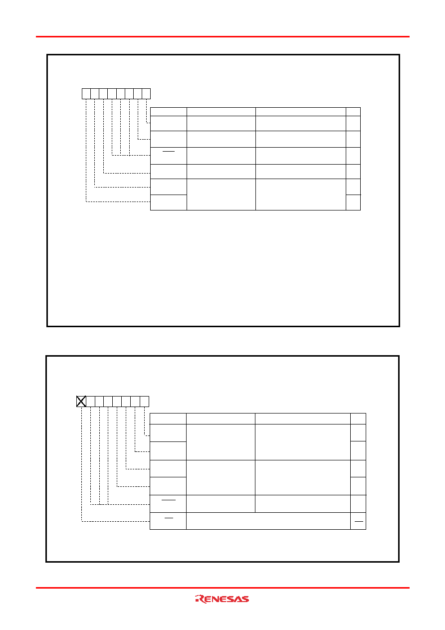
Figure 7.3 CM1 Register
Figure 7.4 ROCR Register
b7 b6 b5 b4 b3
b2 b1 b0
RW
ROCR0
ROCR1
On-chip Oscillator Control Register(1)
Bit Name
Function
Bit Symbol
Frequency select bits
RW
Reserved bit
00
0
0 0: f1 (ROC)
0 1: f2 (ROC)
1 0: Do not set to this value
1 1: f3 (ROC)
b1 b0
ROCR2
ROCR3
Divider select bits
RW
0 0: Do not set to this value
0 1: divide by 2
1 0: divide by 4
1 1: divide by 8
b3 b2
NOTE:
1. Write to this register after setting the PRC0 bit in the PRCR register to 1 (write enable).
(b6-b4)
Set to 0
(b7)
RW
Nothing is assigned. When write, set to 0.
When read, the content is undefined
Symbol
Address
After Reset
ROCR
025C16
X00001012
System Clock Control Register 1 (1)
Symbol
Address
After Reset
CM1
000716
001000002
Bit Name
Function
Bit Symbol
b7 b6 b5 b4 b3 b2 b1 b0
CM10
All clock stop control bit
(4, 6)
0 : Clock on
1 : All clocks off (stop mode)
CM15
XIN-XOUT drive capacity
select bit (2)
0 : LOW
1 : HIGH
RW
CM16
CM17
Reserved bit
Set to
0
Main clock division
select bits (3)
0 0 : No division mode
0 1 : Division by 2 mode
1 0 : Division by 4 mode
1 1 : Division by 16 mode
b7 b6
0
00
CM11
System clock select bit 1
(6, 7)
0 : Main clock
1 : PLL clock (5)
RW
(b4-b2)
NOTES:
1. Write to this register after setting the PRC0 bit in the PRCR register to 1 (write enable).
2. When entering stop mode from high or middle speed mode, or when the CM05 bit is set to 1 (main clock
turned off) in low speed mode, the CM15 bit is set to 1 (drive capability high).
3. Effective when the CM06 bit is 0 (bits CM16 and CM17 enable).
4. If the CM10 bit is 1 (stop mode), XOUT goes “H” and the internal feedback resistor is disconnected. The XCIN
and XCOUT pins are placed in the high-impedance state. When the CM11 bit is set to 1 (PLL clock), or the
CM20 bit in the CM2 register is set to 1 (oscillation stop, re-oscillation detection function enabled), do not set
the CM10 bit to 1.
5. After setting the PLC07 bit in the PLC0 register to 1 (PLL operation), wait until tsu (PLL) elapses before setting
the CM11 bit to 1 (PLL clock).
6. When the PM21 bit in the PM2 register is set to 1 (clock modification disable), writing to bits CM10, CM11 has
no effect. When the PM22 bit in the PM2 register is set to 1 (watchdog timer count source is on-chip oscillator
clock), writing to the CM10 bit has no effect.
7. Effective when CM07 bit is 0 and CM21 bit is 0 .
相關(guān)PDF資料 |
PDF描述 |
|---|---|
| M30280FATHP | 16-BIT, FLASH, 20 MHz, MICROCONTROLLER, PQFP80 |
| M30281MAV-XXXHP | 16-BIT, MROM, 20 MHz, MICROCONTROLLER, PQFP64 |
| M30280MA-XXXHP-U3 | 16-BIT, MROM, 20 MHz, MICROCONTROLLER, PQFP80 |
| M302801FCHP-U3 | 16-BIT, FLASH, 20 MHz, MICROCONTROLLER, PQFP80 |
| M30281F8HP-U3 | 16-BIT, FLASH, 20 MHz, MICROCONTROLLER, PQFP64 |
相關(guān)代理商/技術(shù)參數(shù) |
參數(shù)描述 |
|---|---|
| M30281M8-XXXHP | 制造商:RENESAS 制造商全稱:Renesas Technology Corp 功能描述:16-BIT SINGLE-CHIP MICROCOMPUTER M16C FAMILY / M16C/Tiny SERIES |
| M30281MA-XXXHP | 制造商:RENESAS 制造商全稱:Renesas Technology Corp 功能描述:16-BIT SINGLE-CHIP MICROCOMPUTER M16C FAMILY / M16C/Tiny SERIES |
| M30281MC-XXXHP | 制造商:RENESAS 制造商全稱:Renesas Technology Corp 功能描述:16-BIT SINGLE-CHIP MICROCOMPUTER M16C FAMILY / M16C/Tiny SERIES |
| M3028BT-EPB | 制造商:Renesas Electronics Corporation 功能描述:DEV EMULATOR PERSONALITY KIT M16C/26A/28 - Trays |
| M30290FAHP | 制造商:RENESAS 制造商全稱:Renesas Technology Corp 功能描述:RENESAS MCU M16C FAMILY / M16C/Tiny SERIES |
發(fā)布緊急采購,3分鐘左右您將得到回復(fù)。