- 您現(xiàn)在的位置:買賣IC網(wǎng) > PDF目錄11035 > LTC6603IUF#PBF (Linear Technology)IC FILTER LOWPASS 24-QFN PDF資料下載
參數(shù)資料
| 型號(hào): | LTC6603IUF#PBF |
| 廠商: | Linear Technology |
| 文件頁(yè)數(shù): | 20/24頁(yè) |
| 文件大?。?/td> | 0K |
| 描述: | IC FILTER LOWPASS 24-QFN |
| 標(biāo)準(zhǔn)包裝: | 91 |
| 濾波器類型: | 低通 |
| 頻率 - 截止或中心: | 80MHz |
| 濾波器數(shù): | 2 |
| 濾波器階數(shù): | 9th |
| 電源電壓: | 2.7 V ~ 3.6 V |
| 安裝類型: | 表面貼裝 |
| 封裝/外殼: | 24-WFQFN 裸露焊盤 |
| 供應(yīng)商設(shè)備封裝: | 24-QFN 裸露焊盤(4x4) |
| 包裝: | 管件 |
| 產(chǎn)品目錄頁(yè)面: | 1323 (CN2011-ZH PDF) |
第1頁(yè)第2頁(yè)第3頁(yè)第4頁(yè)第5頁(yè)第6頁(yè)第7頁(yè)第8頁(yè)第9頁(yè)第10頁(yè)第11頁(yè)第12頁(yè)第13頁(yè)第14頁(yè)第15頁(yè)第16頁(yè)第17頁(yè)第18頁(yè)第19頁(yè)當(dāng)前第20頁(yè)第21頁(yè)第22頁(yè)第23頁(yè)第24頁(yè)
LTC6603
5
6603fa
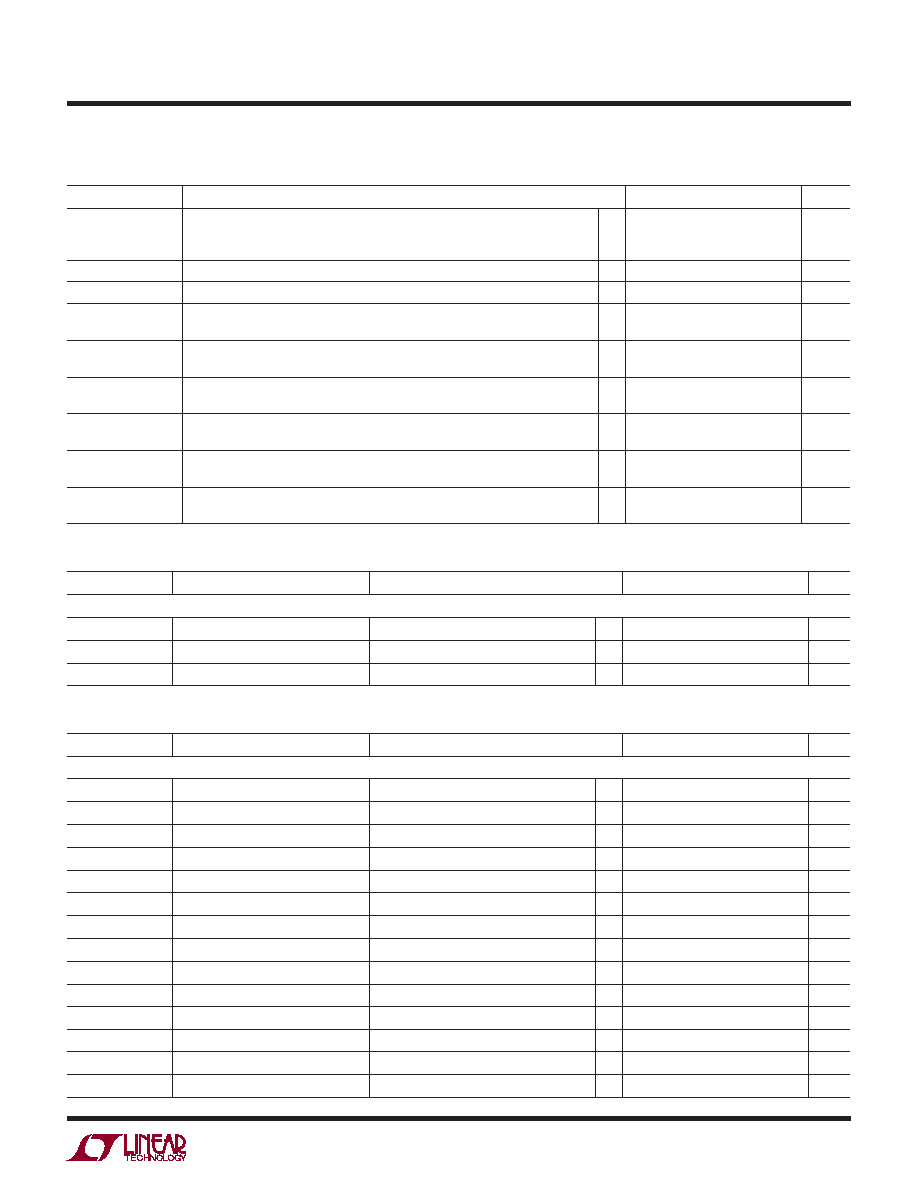
ELECTRICAL CHARACTERISTICS The l denotes the specications which apply over the full operating
temperature range, otherwise specications are at TA = 25°C. V+A = V+D = V+IN = 3V, VICM = VOCM = 1.5V, Gain = 0dB, lowpass cutoff =
2.5MHz, internal clocking with RBIAS = 30.9k unless otherwise noted.
PARAMETER
CONDITIONS
MIN
TYP
MAX
UNITS
CLKIO Pin Low Level
Output Voltage
V+A = V+D = 3V, CLKCNTL = 3V
IOL = 1mA
IOL = 4mA
0.05
0.1
V
CLKIO Pin Rise Time
V+A = V+D = CLKCNTL = 3V, CLOAD = 5pF
0.3
ns
CLKIO Pin Fall Time
V+A = V+D = CLKCNTL = 3V, CLOAD = 5pF
0.3
ns
SER High Level
Input Voltage
Pin 17
l
V+D – 0.3
V
SER Low Level
Input Voltage
Pin 17
l
0.3
V
SER Input Current
Pin 17 = 0V (Note 6)
Pin 17 = V+D
l
–10
2
μA
CLKCNTL High Level
Input Voltage
Pin 5
l
V+D – 0.5
V
CLKCNTL Low Level
Input Voltage
Pin 5
0.5
V
CLKCNTL Input
Current
CLKCNTL = 0V (Note 6)
CLKCNTL = V+D
l
–25
–15
15
25
μA
Pin Programmable Control Mode Specications. Specications apply to Pins 6, 9, 21 and 22 in pin programmable control mode.
SYMBOL
PARAMETER
CONDITIONS
MIN
TYP
MAX
UNITS
V+D = 2.7V to 3.6V
VIH
Digital Input High Voltage
Pins 6, 9, 21, 22
l
2V
VIL
Digital Input Low Voltage
Pins 6, 9, 21, 22
l
0.8
V
IIN
Digital Input Current
Pins 6, 9, 21, 22 (Note 6)
l
–1
1
μA
Serial Port DC and Timing Specications. Specications apply to Pins 6, 9-11, and 21 in serial programming mode.
SYMBOL
PARAMETER
CONDITIONS
MIN
TYP
MAX
UNITS
V+D = 2.7V to 3.6V
VIH
Digital Input High Voltage
Pins 6, 9, 10
l
2V
VIL
Digital Input Low Voltage
Pins 6, 9, 10
l
0.8
V
IIN
Digital Input Current
Pins 6, 9, 10 (Note 6)
l
–1
1
μA
VOH
Digital Output High Voltage
Pins 11, 21 Sourcing 500μA
l VSUPPLY – 0.3
V
VOL
Digital Output Low Voltage
Pins 11, 21 Sinking 500μA
l
0.3
V
t1 (Note 5)
SDI Valid to SCLK Setup
l
60
ns
t2 (Note 5)
SDI Valid to SCLK Hold
l
0ns
t3
SCLK Low
l
100
ns
t4
SCLK High
l
100
ns
t5
CS Pulse Width
l
60
ns
t6 (Note 5)
LSB SCLK to CS
l
60
ns
t7 (Note 5)
CS Low to SCLK
l
30
ns
t8
SDO Output Delay
CL = 15pF
l
125
ns
t9 (Note 5)
SCLK Low to CS Low
l
0ns
相關(guān)PDF資料 |
PDF描述 |
|---|---|
| VE-JWH-IW-B1 | CONVERTER MOD DC/DC 52V 100W |
| VE-JWF-IW-B1 | CONVERTER MOD DC/DC 72V 100W |
| LTC1064CSW#PBF | IC FILTR BUILDNG BLK QUAD 24SOIC |
| VE-JWD-IW-B1 | CONVERTER MOD DC/DC 85V 100W |
| QPI-12LZ | FILTER VI CHIP 48V 7A LGA |
相關(guān)代理商/技術(shù)參數(shù) |
參數(shù)描述 |
|---|---|
| LTC6603IUF-TRPBF | 制造商:LINER 制造商全稱:Linear Technology 功能描述:Dual Adjustable Lowpass Filter |
| LTC6604CUFF-10-TRPBF | 制造商:LINER 制造商全稱:Linear Technology 功能描述:Dual Very Low Noise, Differential Amplifi er and 10MHz Lowpass Filter |
| LTC6604CUFF-15-TRPBF | 制造商:LINER 制造商全稱:Linear Technology 功能描述:Dual Very Low Noise, Differential Amplifi er and 15MHz Lowpass Filter |
| LTC6604IUFF-10-TRPBF | 制造商:LINER 制造商全稱:Linear Technology 功能描述:Dual Very Low Noise, Differential Amplifi er and 10MHz Lowpass Filter |
| LTC6604IUFF-15-TRPBF | 制造商:LINER 制造商全稱:Linear Technology 功能描述:Dual Very Low Noise, Differential Amplifi er and 15MHz Lowpass Filter |
發(fā)布緊急采購(gòu),3分鐘左右您將得到回復(fù)。