- 您現(xiàn)在的位置:買賣IC網(wǎng) > PDF目錄384633 > LTC1649 (Linear Technology Corporation) Low Power Timer 8-SOIC -40 to 85 PDF資料下載
參數(shù)資料
| 型號: | LTC1649 |
| 廠商: | Linear Technology Corporation |
| 英文描述: | Low Power Timer 8-SOIC -40 to 85 |
| 中文描述: | 3.3V輸入高功率降壓型開關(guān)穩(wěn)壓控制器 |
| 文件頁數(shù): | 7/16頁 |
| 文件大?。?/td> | 201K |
| 代理商: | LTC1649 |
7
LTC1649
APPLICATIO
S I
N
FOR
ATIO
U
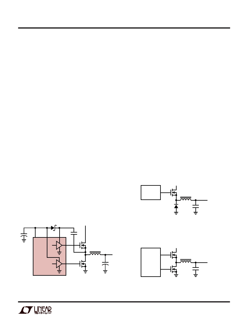
MOSFET Gate Drive
The LTC1649 is designed to operate from supplies as low
as 2.7V while using standard 5V logic-level N-channel
external MOSFETs. This poses somewhat of a challenge—
from as little as 2.7V, the LTC1649 must provide a 0V to
5V signal to the lower MOSFET, Q2, while the upper
MOSFET, Q1, requires a gate drive signal that swings from
0V to (V
IN
+ 5V). The LTC1649 addresses this situation
with two specialized circuits. An onboard charge pump
boosts the input voltage at V
IN
to a regulated 5V at CP
OUT
.
This 5V supply is used to power the PV
CC2
pin, which in
turn supplies 5V gate drive to Q2. This 5V supply is also
used to power the V
CC
pin, which allows the internal drive
circuitry to interface to the boosted driver supplies.
Gate drive for the top N-channel MOSFET, Q1, is supplied
by PV
CC1
. This supply must reach V
IN
+ 5V while Q1 is on.
Conveniently, the switching node at the source of Q1 rises
to V
IN
whenever Q1 is on. The LTC1649 uses this fact to
generate the required voltage at PV
CC1
with a simple
external charge pump as shown in Figure 2. This circuit
charges the flying capacitor C2 to the 5V level at CP
OUT
when the switching node is low. As the top MOSFET turns
on, the switching node begins to rise to V
IN
, and the PV
CC1
is pulled up to V
IN
+ 5V by C2. The 93% maximum duty
cycle (typical) means the switching node at the source of
Q1 will return to ground during at least 7% of each cycle,
ensuring that the charge pump will always provide ad-
equate gate drive to Q1.
W
U
Synchronous Operation
The LTC1649 uses a synchronous switching architecture,
with MOSFET Q2 taking the place of the diode in a classic
buck circuit (Figure 3). This improves efficiency by reduc-
ing the voltage drop and the resultant power dissipation
across Q2 to V
ON
= (I)(R
DS(ON)(Q2)
), usually much lower
than V
F
of the diode in the classical circuit. This more than
offsets the additional gate drive required by the second
MOSFET, allowing the LTC1649 to achieve efficiencies in
the mid-90% range for a wide range of load currents.
Another feature of the synchronous architecture is that
unlike a diode, Q2 can conduct current in either direction.
This allows the output of a typical LTC1649 circuit to sink
current as well as sourcing it while remaining in regula-
tion. The ability to sink current at the output allows the
LTC1649 to be used with reactive or other nonconventional
loads that may supply current to the regulator as well as
drawing current from it.
Figure 2. PV
CC1
Charge Pump
Figure 3b. Synchronous Buck Architecture
Figure 3a. Classical Buck Architecture
LTC1649
CP
OUT
PV
CC2
PV
CC1
Q1
L1
Q2
G1
G2
V
IN
C
OUT
V
OUT
1649 F02
+
10
μ
F
+
1
μ
F
D
CP
Q1
D1
V
IN
V
OUT
CONTROLLER
1649 F03a
Q1
V
IN
V
OUT
CONTROLLER
Q2
1649 F03b
相關(guān)PDF資料 |
PDF描述 |
|---|---|
| LTC1649CS | Low Power Timer 8-SOIC -40 to 85 |
| LTC1666 | 12-Bit, 14-Bit, 16-Bit, 50Msps DACs |
| LTC1666CG | 12-Bit, 14-Bit, 16-Bit, 50Msps DACs |
| LTC1666IG | 12-Bit, 14-Bit, 16-Bit, 50Msps DACs |
| LTC1667 | 12-Bit, 14-Bit, 16-Bit, 50Msps DACs |
相關(guān)代理商/技術(shù)參數(shù) |
參數(shù)描述 |
|---|---|
| LTC1649CS | 功能描述:IC REG CTRLR BUCK PWM VM 16-SOIC RoHS:否 類別:集成電路 (IC) >> PMIC - 穩(wěn)壓器 - DC DC 切換控制器 系列:- 標(biāo)準(zhǔn)包裝:4,500 系列:PowerWise® PWM 型:控制器 輸出數(shù):1 頻率 - 最大:1MHz 占空比:95% 電源電壓:2.8 V ~ 5.5 V 降壓:是 升壓:無 回掃:無 反相:無 倍增器:無 除法器:無 Cuk:無 隔離:無 工作溫度:-40°C ~ 125°C 封裝/外殼:6-WDFN 裸露焊盤 包裝:帶卷 (TR) 配用:LM1771EVAL-ND - BOARD EVALUATION LM1771 其它名稱:LM1771SSDX |
| LTC1649CS#PBF | 功能描述:IC REG CTRLR BUCK PWM VM 16-SOIC RoHS:是 類別:集成電路 (IC) >> PMIC - 穩(wěn)壓器 - DC DC 切換控制器 系列:- 特色產(chǎn)品:LM3753/54 Scalable 2-Phase Synchronous Buck Controllers 標(biāo)準(zhǔn)包裝:1 系列:PowerWise® PWM 型:電壓模式 輸出數(shù):1 頻率 - 最大:1MHz 占空比:81% 電源電壓:4.5 V ~ 18 V 降壓:是 升壓:無 回掃:無 反相:無 倍增器:無 除法器:無 Cuk:無 隔離:無 工作溫度:-5°C ~ 125°C 封裝/外殼:32-WFQFN 裸露焊盤 包裝:Digi-Reel® 產(chǎn)品目錄頁面:1303 (CN2011-ZH PDF) 其它名稱:LM3754SQDKR |
| LTC1649CS#TR | 功能描述:IC REG CTRLR BUCK PWM VM 16-SOIC RoHS:否 類別:集成電路 (IC) >> PMIC - 穩(wěn)壓器 - DC DC 切換控制器 系列:- 標(biāo)準(zhǔn)包裝:2,500 系列:- PWM 型:電流模式 輸出數(shù):1 頻率 - 最大:500kHz 占空比:96% 電源電壓:4 V ~ 36 V 降壓:無 升壓:是 回掃:無 反相:無 倍增器:無 除法器:無 Cuk:無 隔離:無 工作溫度:-40°C ~ 125°C 封裝/外殼:24-WQFN 裸露焊盤 包裝:帶卷 (TR) |
| LTC1649CS#TRPBF | 功能描述:IC REG CTRLR BUCK PWM VM 16-SOIC RoHS:否 類別:集成電路 (IC) >> PMIC - 穩(wěn)壓器 - DC DC 切換控制器 系列:- 標(biāo)準(zhǔn)包裝:2,500 系列:- PWM 型:電流模式 輸出數(shù):1 頻率 - 最大:500kHz 占空比:96% 電源電壓:4 V ~ 36 V 降壓:無 升壓:是 回掃:無 反相:無 倍增器:無 除法器:無 Cuk:無 隔離:無 工作溫度:-40°C ~ 125°C 封裝/外殼:24-WQFN 裸露焊盤 包裝:帶卷 (TR) |
| LTC1649IS | 功能描述:IC REG CTRLR BUCK PWM VM 16-SOIC RoHS:否 類別:集成電路 (IC) >> PMIC - 穩(wěn)壓器 - DC DC 切換控制器 系列:- 標(biāo)準(zhǔn)包裝:4,500 系列:PowerWise® PWM 型:控制器 輸出數(shù):1 頻率 - 最大:1MHz 占空比:95% 電源電壓:2.8 V ~ 5.5 V 降壓:是 升壓:無 回掃:無 反相:無 倍增器:無 除法器:無 Cuk:無 隔離:無 工作溫度:-40°C ~ 125°C 封裝/外殼:6-WDFN 裸露焊盤 包裝:帶卷 (TR) 配用:LM1771EVAL-ND - BOARD EVALUATION LM1771 其它名稱:LM1771SSDX |
發(fā)布緊急采購,3分鐘左右您將得到回復(fù)。