- 您現(xiàn)在的位置:買(mǎi)賣(mài)IC網(wǎng) > PDF目錄384633 > LTC1649 (Linear Technology Corporation) Low Power Timer 8-SOIC -40 to 85 PDF資料下載
參數(shù)資料
| 型號(hào): | LTC1649 |
| 廠商: | Linear Technology Corporation |
| 英文描述: | Low Power Timer 8-SOIC -40 to 85 |
| 中文描述: | 3.3V輸入高功率降壓型開(kāi)關(guān)穩(wěn)壓控制器 |
| 文件頁(yè)數(shù): | 12/16頁(yè) |
| 文件大小: | 201K |
| 代理商: | LTC1649 |
第1頁(yè)第2頁(yè)第3頁(yè)第4頁(yè)第5頁(yè)第6頁(yè)第7頁(yè)第8頁(yè)第9頁(yè)第10頁(yè)第11頁(yè)當(dāng)前第12頁(yè)第13頁(yè)第14頁(yè)第15頁(yè)第16頁(yè)
12
LTC1649
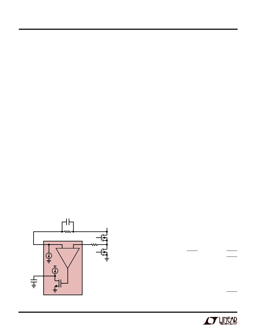
The LTC1649 detects the output current by watching the
voltage at I
FB
while Q1 is ON. The I
LIM
amplifier compares
this voltage to the voltage at I
MAX
(Figure 7). In the ON
state, Q1 has a known resistance; by calculating back-
wards, the voltage generated at I
FB
by the maximum
output current in Q1 can be determined. As I
FB
falls below
I
MAX
, I
LIM
will begin to sink current from the soft start pin,
causing the voltage at SS to fall. As SS falls, it will limit the
output duty cycle, limiting the current at the output.
Eventually the system will reach equilibrium, where the
pull-up current at the SS pin matches the pull-down
current in the I
LIM
amplifier; the LTC1649 will stay in this
state until the overcurrent condition disappears. At this
time I
FB
will rise, I
LIM
will stop sinking current and the
internal pull-up will recharge the soft start capacitor,
restoring normal operation. Note that the I
FB
pin requires
an external 1k series resistor to prevent voltage transients
at the drain of Q2 from damaging internal structures.
The I
LIM
amplifier pulls current out of SS in proportion to
the difference between I
FB
and I
MAX
. Under mild overload
conditions, the SS pin will fall gradually, creating a time
delay before current limit takes effect. Very short, mild
overloads may not trip the current limit circuit at all.
Longer overload conditions will allow the SS pin to reach
a steady level, and the output will remain at a reduced
voltage until the overload is removed. Serious overloads
will generate a larger overdrive at I
LIM
, allowing it to pull SS
down more quickly and preventing damage to the output
components.
The I
LIM
amplifier output is disabled when Q1 is OFF to
prevent the low I
FB
voltage in this condition from activating
the current limit. It is re-enabled a fixed 170ns after Q1
turns on; this allows for the I
FB
node to slew back high and
the I
LIM
amplifier to settle to the correct value. As the
LTC1649 goes deeper into current limit, it will reach a point
where the Q1 on-time needs to be cut to below 170ns to
control the output current. This conflicts with the mini-
mum settling time needed for proper operation of the I
LIM
amplifier. At this point, a secondary current limit circuit
begins to reduce the internal oscillator frequency, length-
ening the off-time of Q1 while the on-time remains con-
stant at 170ns. This further reduces the duty cycle, allow-
ing the LTC1649 to maintain control over the output
current.
Under extreme output overloads or short circuits, the I
LIM
amplifier will pull the SS pin more than 2V below V
CC
in a
single switching cycle, cutting the duty cycle to zero. At
this point all switching stops, the output current decays
through Q2 and the LTC1649 runs a partial soft start cycle
and restarts. If the short is still present the cycle will
repeat. Peak currents can be quite high in this condition,
but the average current is controlled and a properly
designed circuit can withstand short circuits indefinitely
with only moderate heat rise in the output FETs. In addi-
tion, the soft start cycle repeat frequency can drop into the
low kHz range, causing vibrations in the inductor which
provide an audible alarm that something is wrong.
Shutdown
The LTC1649 includes a low power shutdown mode,
controlled by the logic at the SHDN pin. A high at SHDN
allows the part to operate normally. A low level at SHDN
stops all internal switching, pulls COMP and SS to ground
internally and turns Q1 and Q2 off. In shutdown, the
LTC1649 itself will drop below 25
μ
A quiescent current
typically, although off-state leakage in the external MOS-
FETs may cause the total V
IN
current to be somewhat
higher, especially at elevated temperatures. When SHDN
rises again, the LTC1649 will rerun a soft start cycle and
APPLICATIO
S I
N
FOR
ATIO
U
W
U
Figure 7. Current Limit Operation
–
+
I
LIM
LTC1649
1649 F07
R
IMAX
V
IN
I
MAX
I
FB
SS
C
SS
12
μ
A
Q1
Q2
12
μ
A
V
CC
1k
0.1
μ
F
相關(guān)PDF資料 |
PDF描述 |
|---|---|
| LTC1649CS | Low Power Timer 8-SOIC -40 to 85 |
| LTC1666 | 12-Bit, 14-Bit, 16-Bit, 50Msps DACs |
| LTC1666CG | 12-Bit, 14-Bit, 16-Bit, 50Msps DACs |
| LTC1666IG | 12-Bit, 14-Bit, 16-Bit, 50Msps DACs |
| LTC1667 | 12-Bit, 14-Bit, 16-Bit, 50Msps DACs |
相關(guān)代理商/技術(shù)參數(shù) |
參數(shù)描述 |
|---|---|
| LTC1649CS | 功能描述:IC REG CTRLR BUCK PWM VM 16-SOIC RoHS:否 類(lèi)別:集成電路 (IC) >> PMIC - 穩(wěn)壓器 - DC DC 切換控制器 系列:- 標(biāo)準(zhǔn)包裝:4,500 系列:PowerWise® PWM 型:控制器 輸出數(shù):1 頻率 - 最大:1MHz 占空比:95% 電源電壓:2.8 V ~ 5.5 V 降壓:是 升壓:無(wú) 回掃:無(wú) 反相:無(wú) 倍增器:無(wú) 除法器:無(wú) Cuk:無(wú) 隔離:無(wú) 工作溫度:-40°C ~ 125°C 封裝/外殼:6-WDFN 裸露焊盤(pán) 包裝:帶卷 (TR) 配用:LM1771EVAL-ND - BOARD EVALUATION LM1771 其它名稱(chēng):LM1771SSDX |
| LTC1649CS#PBF | 功能描述:IC REG CTRLR BUCK PWM VM 16-SOIC RoHS:是 類(lèi)別:集成電路 (IC) >> PMIC - 穩(wěn)壓器 - DC DC 切換控制器 系列:- 特色產(chǎn)品:LM3753/54 Scalable 2-Phase Synchronous Buck Controllers 標(biāo)準(zhǔn)包裝:1 系列:PowerWise® PWM 型:電壓模式 輸出數(shù):1 頻率 - 最大:1MHz 占空比:81% 電源電壓:4.5 V ~ 18 V 降壓:是 升壓:無(wú) 回掃:無(wú) 反相:無(wú) 倍增器:無(wú) 除法器:無(wú) Cuk:無(wú) 隔離:無(wú) 工作溫度:-5°C ~ 125°C 封裝/外殼:32-WFQFN 裸露焊盤(pán) 包裝:Digi-Reel® 產(chǎn)品目錄頁(yè)面:1303 (CN2011-ZH PDF) 其它名稱(chēng):LM3754SQDKR |
| LTC1649CS#TR | 功能描述:IC REG CTRLR BUCK PWM VM 16-SOIC RoHS:否 類(lèi)別:集成電路 (IC) >> PMIC - 穩(wěn)壓器 - DC DC 切換控制器 系列:- 標(biāo)準(zhǔn)包裝:2,500 系列:- PWM 型:電流模式 輸出數(shù):1 頻率 - 最大:500kHz 占空比:96% 電源電壓:4 V ~ 36 V 降壓:無(wú) 升壓:是 回掃:無(wú) 反相:無(wú) 倍增器:無(wú) 除法器:無(wú) Cuk:無(wú) 隔離:無(wú) 工作溫度:-40°C ~ 125°C 封裝/外殼:24-WQFN 裸露焊盤(pán) 包裝:帶卷 (TR) |
| LTC1649CS#TRPBF | 功能描述:IC REG CTRLR BUCK PWM VM 16-SOIC RoHS:否 類(lèi)別:集成電路 (IC) >> PMIC - 穩(wěn)壓器 - DC DC 切換控制器 系列:- 標(biāo)準(zhǔn)包裝:2,500 系列:- PWM 型:電流模式 輸出數(shù):1 頻率 - 最大:500kHz 占空比:96% 電源電壓:4 V ~ 36 V 降壓:無(wú) 升壓:是 回掃:無(wú) 反相:無(wú) 倍增器:無(wú) 除法器:無(wú) Cuk:無(wú) 隔離:無(wú) 工作溫度:-40°C ~ 125°C 封裝/外殼:24-WQFN 裸露焊盤(pán) 包裝:帶卷 (TR) |
| LTC1649IS | 功能描述:IC REG CTRLR BUCK PWM VM 16-SOIC RoHS:否 類(lèi)別:集成電路 (IC) >> PMIC - 穩(wěn)壓器 - DC DC 切換控制器 系列:- 標(biāo)準(zhǔn)包裝:4,500 系列:PowerWise® PWM 型:控制器 輸出數(shù):1 頻率 - 最大:1MHz 占空比:95% 電源電壓:2.8 V ~ 5.5 V 降壓:是 升壓:無(wú) 回掃:無(wú) 反相:無(wú) 倍增器:無(wú) 除法器:無(wú) Cuk:無(wú) 隔離:無(wú) 工作溫度:-40°C ~ 125°C 封裝/外殼:6-WDFN 裸露焊盤(pán) 包裝:帶卷 (TR) 配用:LM1771EVAL-ND - BOARD EVALUATION LM1771 其它名稱(chēng):LM1771SSDX |
發(fā)布緊急采購(gòu),3分鐘左右您將得到回復(fù)。