- 您現(xiàn)在的位置:買賣IC網(wǎng) > PDF目錄44985 > LT3579IUFD-1#PBF (LINEAR TECHNOLOGY CORP) SWITCHING REGULATOR, PQCC20 PDF資料下載
參數(shù)資料
| 型號(hào): | LT3579IUFD-1#PBF |
| 廠商: | LINEAR TECHNOLOGY CORP |
| 元件分類: | 穩(wěn)壓器 |
| 英文描述: | SWITCHING REGULATOR, PQCC20 |
| 封裝: | 4 X 5 MM, LEAD FREE, PLASTIC, MO-220, QFN-20 |
| 文件頁(yè)數(shù): | 18/40頁(yè) |
| 文件大小: | 503K |
| 代理商: | LT3579IUFD-1#PBF |
第1頁(yè)第2頁(yè)第3頁(yè)第4頁(yè)第5頁(yè)第6頁(yè)第7頁(yè)第8頁(yè)第9頁(yè)第10頁(yè)第11頁(yè)第12頁(yè)第13頁(yè)第14頁(yè)第15頁(yè)第16頁(yè)第17頁(yè)當(dāng)前第18頁(yè)第19頁(yè)第20頁(yè)第21頁(yè)第22頁(yè)第23頁(yè)第24頁(yè)第25頁(yè)第26頁(yè)第27頁(yè)第28頁(yè)第29頁(yè)第30頁(yè)第31頁(yè)第32頁(yè)第33頁(yè)第34頁(yè)第35頁(yè)第36頁(yè)第37頁(yè)第38頁(yè)第39頁(yè)第40頁(yè)
LT3579/LT3579-1
25
35791f
appenDix
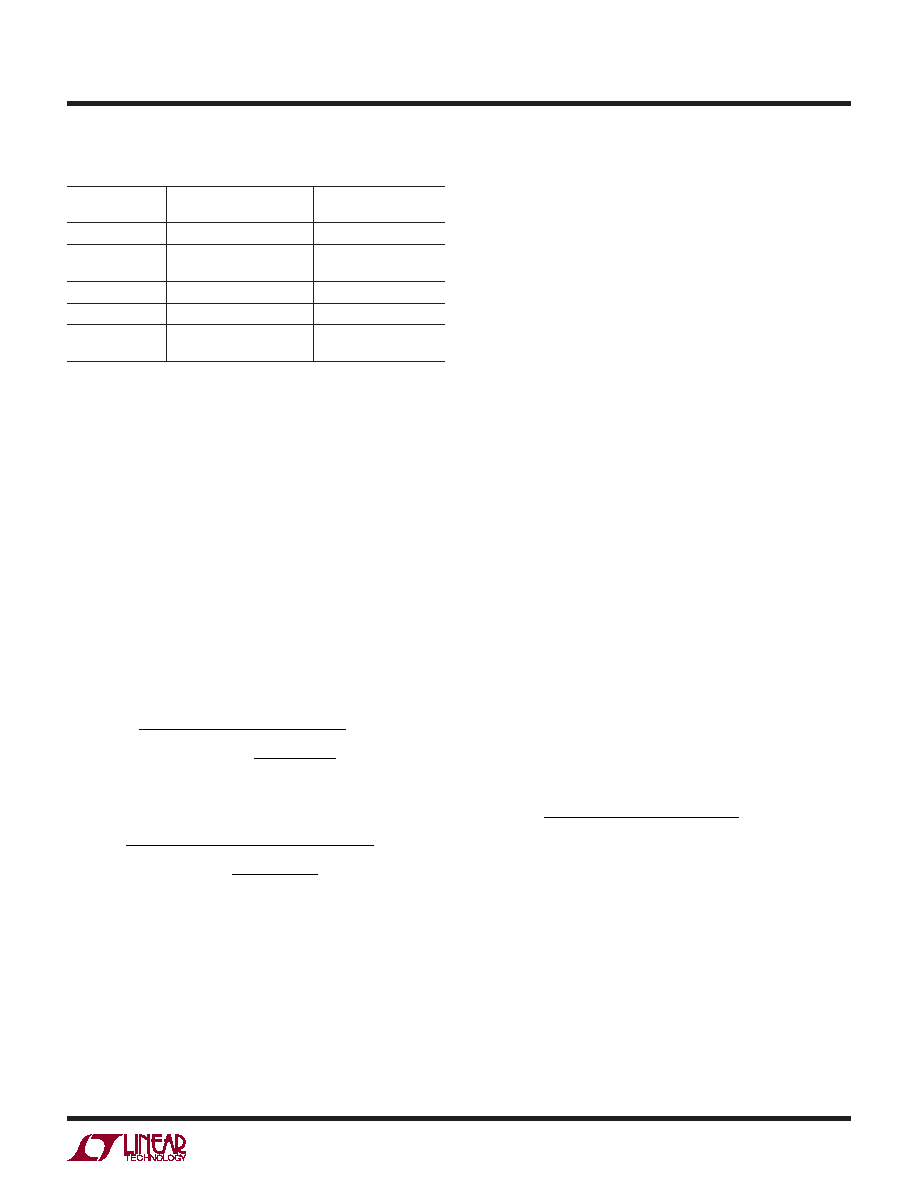
Table 5. Inductor Manufacturers
Vishay
IHLP-2020BZ-01 and
IHLP-2525CZ-01 Series
www.vishay.com
Coilcraft
XLP, MLC and MSS Series www.coilcraft.com
Cooper Bussmann DRQ125 and DRQ127
Series
www.cooperbussmann.
com
Sumida
CDRH series
www.sumida.com
TDK
RLF and SLF series
www.tdk.com
Würth
WE-PD, WE-PDF, WE-HC
and WE-DD Series
www.we-online.com
Minimum Inductance
Although there can be a tradeoff with efficiency, it is often
desirable to minimize board space by choosing smaller
inductors. When choosing an inductor, there are three
conditionsthatlimittheminimuminductance;(1)providing
adequate load current, (2) avoidance of subharmonic
oscillation, and (3) supplying a minimum ripple current
to avoid false tripping of the current comparator.
Adequate Load Current
Smallvalueinductorsresultinincreasedripplecurrentsand
thus, due to the limited peak switch current, decrease the
average current that can be provided to the load. In order
to provide adequate load current, L should be at least:
LBOOST >
DC
VIN VCESAT
(
)
2
fOSC IPK
VOUT IOUT
VIN η
or
LDUAL >
DC
VIN VCESAT
(
)
2
fOSC IPK
|VOUT |IOUT
VIN η
IOUT
Boost
Topology
SEPIC
or
Inverting
Topologies
where:
LBOOST = L1 for Boost Topologies (see Figure 6)
LDUAL = L1 = L2 for Coupled Dual Inductor
Topologies (see Figures 7 and 8)
LDUAL = L1 || L2 for Uncoupled Dual Inductor
Topologies (see Figures 7 and 8)
DC
= SwitchDutyCycle(seePowerSwitchDuty
Cycle section in Appendix)
IPK
= Maximum Peak Switch Current; Should
Not Exceed 6A for a Combined SW1 +
SW2 Current or 3.4A of SW1 Current (see
Electrical Characteristics section.)
η
= Power Conversion Efficiency (typically 90%
for Boost and 85% for Dual Inductor
Topologies at high currents)
fOSC
= Switching Frequency
IOUT
= Maximum Output Current
Negative values of LBOOST or LDUAL indicate that the
output load current, IOUT, exceeds the switch current limit
capability of the LT3579.
Avoiding Sub-Harmonic Oscillations
The LT3579’s internal slope compensation circuit will
prevent sub-harmonic oscillations that can occur when
the duty cycle is greater than 50%, provided that the
inductance exceeds a minimum value. In applications that
operate with duty cycles greater than 50%, the inductance
must be at least:
LMIN =
VIN VCESAT
(
) 2DC1
(
)
4A
fOSC 1DC
(
)
where:
LMIN = L1 for Boost Topologies (see Figure 6)
LMIN = L1 = L2 for Coupled Dual Inductor
Topologies (see Figures 7 and 8)
LMIN = L1 || L2 for Uncoupled Dual Inductor
Topologies (see Figures 7 and 8)
相關(guān)PDF資料 |
PDF描述 |
|---|---|
| LT3579IFE#TRPBF | SWITCHING REGULATOR, PDSO20 |
| LT3579EFE#TRPBF | SWITCHING REGULATOR, PDSO20 |
| LT3579EUFD-1#PBF | SWITCHING REGULATOR, PQCC20 |
| LT3579EFE-1#TRPBF | SWITCHING REGULATOR, PDSO20 |
| LT3579IFE-1#PBF | SWITCHING REGULATOR, PDSO20 |
相關(guān)代理商/技術(shù)參數(shù) |
參數(shù)描述 |
|---|---|
| LT3579IUFD-1-TRPBF | 制造商:LINER 制造商全稱:Linear Technology 功能描述:6A Boost/Inverting DC/DC Converter with Fault Protection |
| LT3579IUFD-PBF | 制造商:LINER 制造商全稱:Linear Technology 功能描述:6A Boost/Inverting DC/DC Converter with Fault Protection |
| LT3579IUFD-TRPBF | 制造商:LINER 制造商全稱:Linear Technology 功能描述:6A Boost/Inverting DC/DC Converter with Fault Protection |
| LT3580 | 制造商:LINER 制造商全稱:Linear Technology 功能描述:Boost/Inverting DC/DC Converter with 2A Switch, Soft-Start, and Synchronization |
| LT3580EDD | 制造商:LINER 制造商全稱:Linear Technology 功能描述:Boost/Inverting DC/DC Converter with 2A Switch, Soft-Start, and Synchronization |
發(fā)布緊急采購(gòu),3分鐘左右您將得到回復(fù)。