- 您現(xiàn)在的位置:買賣IC網(wǎng) > PDF目錄384602 > LMC1992 (National Semiconductor Corporation) LMC1992 Digitally-Controlled Stereo Tone and Volume Circuit with Four-Channel Input-Selector PDF資料下載
參數(shù)資料
| 型號(hào): | LMC1992 |
| 廠商: | National Semiconductor Corporation |
| 英文描述: | LMC1992 Digitally-Controlled Stereo Tone and Volume Circuit with Four-Channel Input-Selector |
| 中文描述: | LMC1992數(shù)控立體聲音調(diào)和音量電路四通道輸入選擇 |
| 文件頁數(shù): | 7/14頁 |
| 文件大小: | 260K |
| 代理商: | LMC1992 |
Applications Information
MINIMUM LOAD IMPEDANCE
The LMC1992 employs emitter-follower buffers at pins 8
and 22 (SELECT OUT), 13 and 14 (LEFT FRONT and
REAR OUTPUTs), and 16 and 17 (RIGHT FRONT-and-
REAR OUTPUTs) that buffer output signals. Typical bias
current of 1 mA is used for the SELECT OUTPUT buffers
and 350
m
A for the LEFT-and-RIGHT, FRONT-and-REAR
OUTPUT buffers.
The Electrical Specifications table lists a maximum input sig-
nal of 2.3 V
rms
(3.25 V
peak
) for 1% THD at the SELECT
OUT pins. This distortion level is achieved when the mini-
mum ac load impedance seen by the SELECT OUT pin is
3.25 k
X
(3.25V/1 mA). For the LEFT-and-RIGHT, FRONT-
and-REAR OUTPUTs, the typical maximum output is 1.2
V
rms
(1.55 V
peak
). Therefore, the minimum load impedance
is 4.43 k
X
(1.55 V/0.35 mA). Trying to use a lower imped-
ance results in a clipped output signal. Therefore, the
chance of clipping can be greatly reduced and much lower
distortion levels can be achieved by using load impedances
that are an order of magnitude higher than shown here.
For applications that require dc coupling and the INPUTs
biased to V
a
/2, the minimum load impedance will differ
from that detailed in the above discussion. The emitter fol-
lowers may be potentially operating at high currents be-
cause there is a dc voltage V
a
/2
b
0.7V at the SELECT
OUT pins; dc resistance to ground will result in increased
current flow. Latch-up may occur if the total emitter current
exceeds 5 mA. This current is a combination of the emitter
follower’s 1 mA current source and 4 mA drawn by the ex-
ternal load. Therefore, to prevent this possibility, the mini-
mum dc load impedance should be
V
peak
a
(V
a
/2
b
0.7V)
4 mA
V
peak
e
3.25V
V
a
e
8V
To allow for variations and part tolerances, 2.0 k
X
is a good
choice for this minimum dc load impedance.
e
1638
X
When dc coupling is used at the LEFT-and-RIGHT, FRONT-
and-REAR OUTPUTs, the output emitter followers will be
operating at a nominal dc voltage of V
a
/2
b
2(0.7V).
Latch-up may occur if the total emitter current exceeds
1 mA. This current is a combination of the emitter follower’s
0.35 mA current source and 0.65 mA drawn by the external
load. Therefore, to prevent this possibility, the minimum dc
load impedance should be
V
peak
a
(V
a
/2
b
2(0.7V))
0.65 mA
V
peak
e
3.25V
V
a
e
8V
e
9 k
X
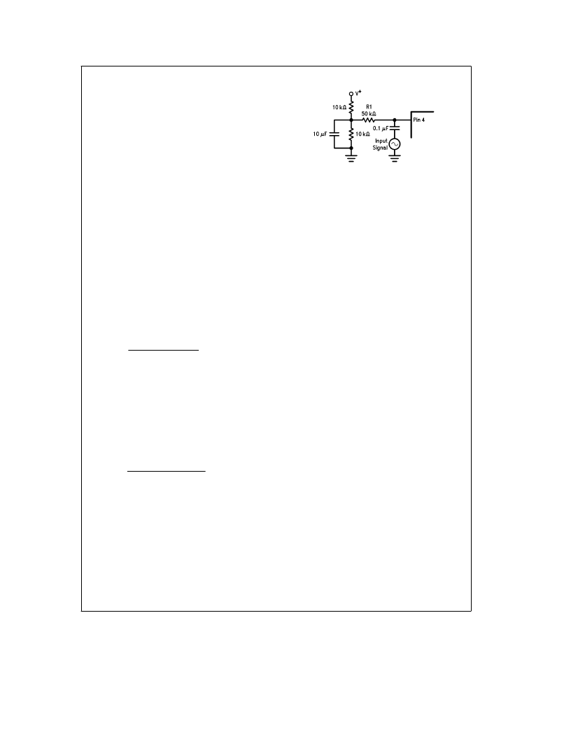
TL/H/10789–20
FIGURE 2. Input Bias Network
To allow for variations and part tolerances, 10 k
X
is a good
choice for this minimum dc load impedance.
INPUT IMPEDANCE
For ac coupled input signals the input impedance value is
determined by bias resistor R1, as shown in Figure 2. A
directly coupled input signal will see an emitter follower’s
nominal input impedance of 2 M
X
.
The SELECT IN pins have an input impedance that varies
with the BASS and TREBLE control settings. The input im-
pedance is 96 k
X
at dc and 27 k
X
at 1 kHz when the con-
trols are set at 0 dB. Minimum input impedance of 28 k
X
at
dc and 24 k
X
at 1 kHz occurs when maximum boost is
selected. At 10 kHz the minimum input impedance, with the
tone controls flat, is 8 k
X
and, with the tone controls at
maximum boost, is 3 k
X
.
STEREO SIGNAL INPUTS
When operating with a single supply voltage, the stereo sig-
nal inputs must be dc biased to one-half of the supply volt-
age, as shown in Figure 2. As an example, with a supply
voltage of 8V, all signal sources should have a dc bias of
4V. The maximum input signal level of 6.5 V
p-p
(for 1%
THD) would then swing from 0.75V to 7.25V. Input-to-input
crosstalk can be minimized by using a separate dc bias cir-
cuit for each stereo input pair.
EXTERNAL SIGNAL PROCESSING
The signal present at the selected input will be available at
the SELECT OUT pins 8 (left) and 22 (right). The dc bias
voltage at those pins will be one base-emitter voltage, ap-
proximately 0.7 V
dc
, below the source because of the inter-
nal emitter follower. Therefore, if the selected input has a
bias of 4.0 V
dc
the dc component at pins 8 and 22 will be
about 3.3 V
dc
.
The LMC1992’s SELECT OUT emitter followers allow addi-
tional signal sources using emitter follower outputs (such as
multiple LMC1992s) to be ‘‘wired-ORed’’ together. When
this feature is in use, the input channel of the LMC1992 not
in use should be set to ‘‘open’’ input codes 01000XX0000 or
01000XX011X.
7
相關(guān)PDF資料 |
PDF描述 |
|---|---|
| LMC1992CCN | LMC1992 Digitally-Controlled Stereo Tone and Volume Circuit with Four-Channel Input-Selector |
| LMC2001 | High Precision, 6MHz Rail-To-Rail Output Operational Amplifier |
| LMC2001ACM5 | High Precision, 6MHz Rail-To-Rail Output Operational Amplifier |
| LMC2001ACM5X | High Precision, 6MHz Rail-To-Rail Output Operational Amplifier |
| LMC2001AIM | High Precision, 6MHz Rail-To-Rail Output Operational Amplifier |
相關(guān)代理商/技術(shù)參數(shù) |
參數(shù)描述 |
|---|---|
| LMC1992CCN | 制造商:NSC 制造商全稱:National Semiconductor 功能描述:LMC1992 Digitally-Controlled Stereo Tone and Volume Circuit with Four-Channel Input-Selector |
| LMC200 | 制造商:Black Box Corporation 功能描述:14 SLOT POWER CHASSIS W/1 POWE |
| LMC2001 | 制造商:NSC 制造商全稱:National Semiconductor 功能描述:High Precision, 6MHz Rail-To-Rail Output Operational Amplifier |
| LMC2001 WAF | 制造商:Texas Instruments 功能描述: |
| LMC2001ACM5 | 制造商:Rochester Electronics LLC 功能描述:- Bulk |
發(fā)布緊急采購(gòu),3分鐘左右您將得到回復(fù)。