- 您現(xiàn)在的位置:買賣IC網(wǎng) > PDF目錄98000 > LM2710MT-ADJ/NOPB (NATIONAL SEMICONDUCTOR CORP) 1.4 A SWITCHING REGULATOR, 1500 kHz SWITCHING FREQ-MAX, PDSO20 PDF資料下載
參數(shù)資料
| 型號(hào): | LM2710MT-ADJ/NOPB |
| 廠商: | NATIONAL SEMICONDUCTOR CORP |
| 元件分類: | 穩(wěn)壓器 |
| 英文描述: | 1.4 A SWITCHING REGULATOR, 1500 kHz SWITCHING FREQ-MAX, PDSO20 |
| 封裝: | TSSOP-20 |
| 文件頁數(shù): | 6/20頁 |
| 文件大?。?/td> | 853K |
| 代理商: | LM2710MT-ADJ/NOPB |
Operation (Continued)
V
OUT =8V, VIN = 2.5V, RL =27
,C
SS = 330nF, T = 4ms/div,
F = 1.25MHz.
Trace:
1) SHDN, 1V/div, DC Coupled
2) I
L, 0.5A/div, DC Coupled
3) V
OUT, 5V/div, DC Coupled
20043480
T
A = 20C
20043481
T
A = 27C
20043482
T
A = 85C
When programming the softstart time externally, simply use
the equation given in the Soft-Start Capacitor section above.
This equation uses the typical room temperature value of the
soft start current, 11A, to set the soft start time.
INTRODUCTION TO COMPENSATION
The LM2710 is a current mode PWM boost converter. The
signal flow of this control scheme has two feedback loops,
one that senses switch current and one that senses output
voltage.
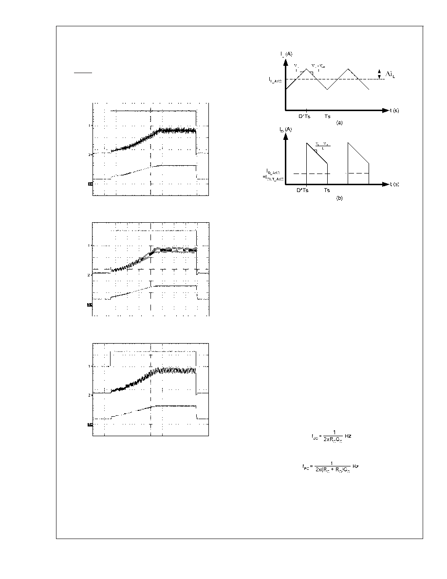
To keep a current programmed control converter stable
above duty cycles of 50%, the inductor must meet certain
criteria. The inductor, along with input and output voltage,
will determine the slope of the current through the inductor
(see Figure 2 (a)). If the slope of the inductor current is too
great, the circuit will be unstable above duty cycles of 50%.
A 10H inductor is recommended for most 600 kHz applica-
tions, while a 4.7H inductor may be used for most 1.25 MHz
applications. If the duty cycle is approaching the maximum of
85%, it may be necessary to increase the inductance by as
much as 2X. See Inductor and Diode Selection for more
detailed inductor sizing.
The LM2710 provides a compensation pin (V
C) to customize
the voltage loop feedback. It is recommended that a series
combination of R
C and CC be used for the compensation
network, as shown in the typical application circuit. For any
given application, there exists a unique combination of R
C
and C
C that will optimize the performance of the LM2710
circuit in terms of its transient response. The series combi-
nation of R
C and CC introduces a pole-zero pair according to
the following equations:
where R
O is the output impedance of the error amplifier,
approximately 1M
. For most applications, performance can
be optimized by choosing values within the range 5k
≤ R
C
≤ 60k (R
C can be up to 200k
if C
C2 is used, see High
Output Capacitor ESR Compensation) and 680pF
≤ C
C
≤
20043405
FIGURE 2. (a) Inductor current. (b) Diode current.
LM2710
www.national.com
14
相關(guān)PDF資料 |
PDF描述 |
|---|---|
| LM2984MDC | 1-CHANNEL POWER SUPPLY SUPPORT CKT, UUC |
| LM3207TL/NOPB | 1.2 A SWITCHING REGULATOR, 2300 kHz SWITCHING FREQ-MAX, PBGA9 |
| LM3218SE | SWITCHING REGULATOR, DSO8 |
| LM3350MWC | SWITCHED CAPACITOR CONVERTER, 1100 kHz SWITCHING FREQ-MAX, UUC |
| LM336BZ-5.0/NOPB | 1-OUTPUT TWO TERM VOLTAGE REFERENCE, 5 V, PBCY3 |
相關(guān)代理商/技術(shù)參數(shù) |
參數(shù)描述 |
|---|---|
| LM2710MTX-ADJ | 制造商:NSC 制造商全稱:National Semiconductor 功能描述:Step-up PWM DC/DC Converter Integrated with 5 Buffers |
| LM2711 | 制造商:NSC 制造商全稱:National Semiconductor 功能描述:TFT Panel Module |
| LM2711A-ADJ WAF | 制造商:Texas Instruments 功能描述: |
| LM2711MT-ADJ | 制造商:NSC 制造商全稱:National Semiconductor 功能描述:TFT Panel Module |
| LM2711MTX-ADJ | 制造商:NSC 制造商全稱:National Semiconductor 功能描述:TFT Panel Module |
發(fā)布緊急采購,3分鐘左右您將得到回復(fù)。