- 您現(xiàn)在的位置:買(mǎi)賣IC網(wǎng) > PDF目錄369756 > LH28F160BJHG-BTLZ3 EEPROM|FLASH|1MX16|CMOS|BGA|48PIN|PLASTIC PDF資料下載
參數(shù)資料
| 型號(hào): | LH28F160BJHG-BTLZ3 |
| 英文描述: | EEPROM|FLASH|1MX16|CMOS|BGA|48PIN|PLASTIC |
| 中文描述: | 的EEPROM | FLASH動(dòng)畫(huà)| 1MX16 |的CMOS | BGA封裝| 48PIN |塑料 |
| 文件頁(yè)數(shù): | 23/56頁(yè) |
| 文件大小: | 373K |
| 代理商: | LH28F160BJHG-BTLZ3 |
第1頁(yè)第2頁(yè)第3頁(yè)第4頁(yè)第5頁(yè)第6頁(yè)第7頁(yè)第8頁(yè)第9頁(yè)第10頁(yè)第11頁(yè)第12頁(yè)第13頁(yè)第14頁(yè)第15頁(yè)第16頁(yè)第17頁(yè)第18頁(yè)第19頁(yè)第20頁(yè)第21頁(yè)第22頁(yè)當(dāng)前第23頁(yè)第24頁(yè)第25頁(yè)第26頁(yè)第27頁(yè)第28頁(yè)第29頁(yè)第30頁(yè)第31頁(yè)第32頁(yè)第33頁(yè)第34頁(yè)第35頁(yè)第36頁(yè)第37頁(yè)第38頁(yè)第39頁(yè)第40頁(yè)第41頁(yè)第42頁(yè)第43頁(yè)第44頁(yè)第45頁(yè)第46頁(yè)第47頁(yè)第48頁(yè)第49頁(yè)第50頁(yè)第51頁(yè)第52頁(yè)第53頁(yè)第54頁(yè)第55頁(yè)第56頁(yè)
LH28F160S5-L/S5H-L
- 23 -
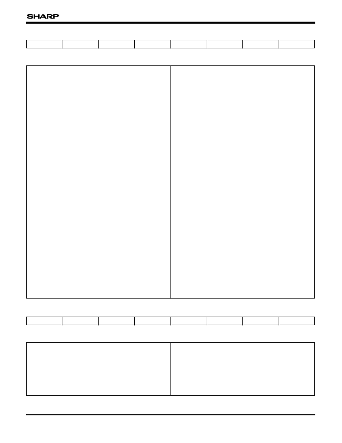
Table 13.1 Status Register Definition
ECBLBS
WSBLBS
5
4
WSMS
7
BESS
6
VPPS
3
WSS
2
DPS
1
R
0
SR.7 = WRITE STATE MACHINE STATUS (WSMS)
1 = Ready
0 = Busy
SR.6 = BLOCK ERASE SUSPEND STATUS (BESS)
1 = Block Erase Suspended
0 = Block Erase in Progress/Completed
SR.5 =
ERASE AND CLEAR BLOCK LOCK-BITS STATUS
(ECBLBS)
1 = Error in Erase or Clear Block Lock-Bits
0 = Successful Erase or Clear Block Lock-Bits
SR.4 =
WRITE AND SET BLOCK LOCK-BIT STATUS
(WSBLBS)
1 = Error in Write or Set Block Lock-Bit
0 = Successful Write or Set Block Lock-Bit
SR.3 = V
PP
STATUS (VPPS)
1 = V
PP
Low Detect, Operation Abort
0 = V
PP
OK
SR.2 = WRITE SUSPEND STATUS (WSS)
1 = Write Suspended
0 = Write in Progress/Completed
SR.1 = DEVICE PROTECT STATUS (DPS)
1 = Block Lock-Bit and/or WP# Lock Detected,
Operation Abort
0 = Unlock
SR.0 =
RESERVED FOR FUTURE ENHANCEMENTS (R)
NOTES :
Check STS or SR.7 to determine block erase, full chip erase,
(multi) word/byte write or block lock-bit configuration
completion.
SR.6-0 are invalid while SR.7 = "0".
If both SR.5 and SR.4 are "1"s after a block erase, full chip
erase, (multi) word/byte write, block lock-bit configuration or
STS configuration attempt, an improper command sequence
was entered.
SR.3 does not provide a continuous indication of V
PP
level.
The WSM interrogates and indicates the V
PP
level only after
block erase, full chip erase, (multi) word/byte write or block
lock-bit configuration command sequences. SR.3 is not
guaranteed to reports accurate feedback only when V
PP
≠
V
PPH1
.
SR.1 does not provide a continuous indication of block lock-bit
values. The WSM interrogates block lock-bit, and WP# only
after block erase, full chip erase, (multi) word/byte write or
block lock-bit configuration command sequences. It informs
the system, depending on the attempted operation, if the block
lock-bit is set and/or WP# is not V
IH
. Reading the block lock
configuration codes after writing the Read Identifier Codes
command indicates block lock-bit status.
SR.0 is reserved for future use and should be masked out
when polling the status register.
Table 13.2 Extended Status Register Definition
R
R
5
4
SMS
7
R
6
R
3
R
2
R
1
R
0
XSR.7 = STATE MACHINE STATUS (SMS)
1 = Multi Word/Byte Write available
0 = Multi Word/Byte Write not available
XSR.6-0 =
RESERVED FOR FUTURE ENHANCEMENTS (R)
NOTES :
After issue a Multi Word/Byte Write command : XSR.7
indicates that a next Multi Word/Byte Write command is
available.
XSR.6-0 are reserved for future use and should be masked
out when polling the extended status register.
相關(guān)PDF資料 |
PDF描述 |
|---|---|
| LH28F160S3B-L10 | Flash ROM |
| LH28F160S3B-L13 | EEPROM|FLASH|1MX16/2MX8|CMOS|BGA|64PIN|PLASTIC |
| LH28F160S3D-L10 | x8/x16 Flash EEPROM |
| LH28F160S3D-L13 | EEPROM|FLASH|1MX16/2MX8|CMOS|SDIP|64PIN|PLASTIC |
| LH28F160S3HB-L10 | x8/x16 Flash EEPROM |
相關(guān)代理商/技術(shù)參數(shù) |
參數(shù)描述 |
|---|---|
| LH28F160BJHG-TTLTD | 制造商:Sharp Microelectronics Corporation 功能描述:16M (1MX16) 3V, BOOT BLOCK, TOP, CSP48, IND, HAZMAT - Trays |
| LH28F160BVE-BTL10 | 制造商:Sharp Microelectronics Corporation 功能描述:16M (2MX8/1MX16) 3V, BOOT BLOCK, BOT, TSOP48, COM - Trays |
| LH28F160BVE-BTL90 | 制造商:Sharp Microelectronics Corporation 功能描述:FLASH PARALLEL 3V/3.3V 16MBIT 2MX8/1MX16 90NS 48TSOP - Trays |
| LH28F160BVE-TTL90 | 制造商:Sharp Microelectronics 功能描述:NOR Flash Parallel 3V/3.3V 16Mbit 2M/1M x 8bit/16bit 90ns 48-Pin TSOP 制造商:Sharp Microelectronics Corporation 功能描述:FLASH PARALLEL 3V/3.3V 16MBIT 2MX8/1MX16 90NS 48TSOP - Trays |
| LH28F160BVHE-TTL90 | 制造商:Sharp Microelectronics Corporation 功能描述:FLASH PARALLEL 3V 16MBIT 2MX8/1MX16 90NS 48TSOP - Trays |
發(fā)布緊急采購(gòu),3分鐘左右您將得到回復(fù)。