- 您現(xiàn)在的位置:買賣IC網(wǎng) > PDF目錄299403 > LFSCM3GA40EP1-5FFN1020I (LATTICE SEMICONDUCTOR CORP) PDF資料下載
參數(shù)資料
| 型號: | LFSCM3GA40EP1-5FFN1020I |
| 廠商: | LATTICE SEMICONDUCTOR CORP |
| 元件分類: | FPGA |
| 中文描述: | FPGA, 216 CLBS, 40000 GATES, 1000 MHz, PBGA1020 |
| 封裝: | 33 X 33 MM, LEAD FREE, FCBGA-1020 |
| 文件頁數(shù): | 218/243頁 |
| 文件大小: | 2674K |
| 代理商: | LFSCM3GA40EP1-5FFN1020I |
第1頁第2頁第3頁第4頁第5頁第6頁第7頁第8頁第9頁第10頁第11頁第12頁第13頁第14頁第15頁第16頁第17頁第18頁第19頁第20頁第21頁第22頁第23頁第24頁第25頁第26頁第27頁第28頁第29頁第30頁第31頁第32頁第33頁第34頁第35頁第36頁第37頁第38頁第39頁第40頁第41頁第42頁第43頁第44頁第45頁第46頁第47頁第48頁第49頁第50頁第51頁第52頁第53頁第54頁第55頁第56頁第57頁第58頁第59頁第60頁第61頁第62頁第63頁第64頁第65頁第66頁第67頁第68頁第69頁第70頁第71頁第72頁第73頁第74頁第75頁第76頁第77頁第78頁第79頁第80頁第81頁第82頁第83頁第84頁第85頁第86頁第87頁第88頁第89頁第90頁第91頁第92頁第93頁第94頁第95頁第96頁第97頁第98頁第99頁第100頁第101頁第102頁第103頁第104頁第105頁第106頁第107頁第108頁第109頁第110頁第111頁第112頁第113頁第114頁第115頁第116頁第117頁第118頁第119頁第120頁第121頁第122頁第123頁第124頁第125頁第126頁第127頁第128頁第129頁第130頁第131頁第132頁第133頁第134頁第135頁第136頁第137頁第138頁第139頁第140頁第141頁第142頁第143頁第144頁第145頁第146頁第147頁第148頁第149頁第150頁第151頁第152頁第153頁第154頁第155頁第156頁第157頁第158頁第159頁第160頁第161頁第162頁第163頁第164頁第165頁第166頁第167頁第168頁第169頁第170頁第171頁第172頁第173頁第174頁第175頁第176頁第177頁第178頁第179頁第180頁第181頁第182頁第183頁第184頁第185頁第186頁第187頁第188頁第189頁第190頁第191頁第192頁第193頁第194頁第195頁第196頁第197頁第198頁第199頁第200頁第201頁第202頁第203頁第204頁第205頁第206頁第207頁第208頁第209頁第210頁第211頁第212頁第213頁第214頁第215頁第216頁第217頁當前第218頁第219頁第220頁第221頁第222頁第223頁第224頁第225頁第226頁第227頁第228頁第229頁第230頁第231頁第232頁第233頁第234頁第235頁第236頁第237頁第238頁第239頁第240頁第241頁第242頁第243頁
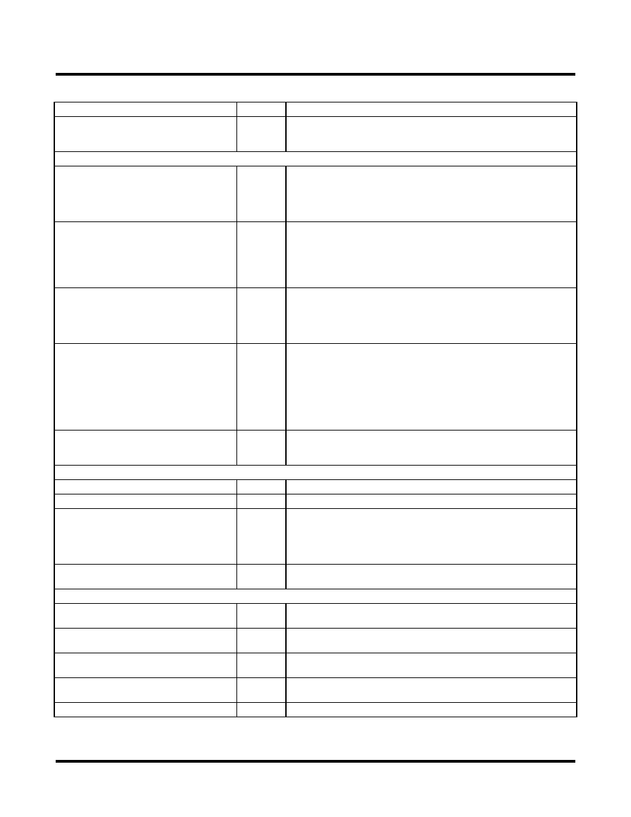
4-2
Pinout Information
Lattice Semiconductor
LatticeSC/M Family Data Sheet
PROBE_GND
—
GND signal - Connected to internal VSS node. Can be used for feed-
back to control an external board power converter. Can be uncon-
nected if not used.
PLL and Clock Functions (Used as user-programmable I/O pins when not in use for PLL, DLL or clock pins.)
[LOC]_PLL[T, C]_FB_[A/B]
I
PLL feedback input. Pull-ups are enabled on input pins during configu-
ration. [LOC] indicates the corner the PLL is located in: ULC (upper
left), URC (upper right), LLC (lower left) and LRC (lower right). [T, C]
indicates whether input is true or complement. [A, B] indicates PLL ref-
erence within the corner.
[LOC]_DLL[T, C]_FB_[C, D, E, F]
I
DLL feedback input. Pull-ups are enabled on input pins during configu-
ration. [LOC] indicates the corner the DLL is located in: ULC (upper
left), URC (upper right), LLC (lower left) and LRC (lower right). [T/C]
indicates whether input is true or complement. [C, D, E, F] indicates
DLL reference within a corner. Note: E and F are only available on the
lower corners.
[LOC]_PLL[T, C]_IN[A/B]
I
PLL reference clock input. Pull-ups are enabled on input pins during
configuration. [LOC] indicates the corner the PLL is located in: ULC
(upper left corner), URC (upper right corner), LLC (lower left corner)
and LRC (lower right corner). [T, C] indicates whether input is true or
complement.[A, B] indicates PLL reference within the corner.
[LOC]_DLL[T, C]_IN[C, D, E, F]
DLL reference clock inputs. Pull-ups are enabled on input pins during
configuration. [LOC] indicates the corner the DLL is located in: ULC
(upper left corner), URC (upper right corner), LLC (lower left corner)
and LRC (lower right corner). [T/C] indicates whether input is true or
complement. [C, D, E, F] indicates DLL reference within a corner.
Note: E and F are only available on the lower corners. PCKLxy_[0:3]
can drive primary clocks, edge clocks, and CLKDIVs. PCLKxy_[4:7]
can only drive edge clocks.
PCLKxy_z
General clock inputs. x indicates whether T (true) or C (complement).
y indicates the I/O bank the clock is associated with. z indicates the
clock number within a bank.
Test and Programming (Dedicated pins. Pull-up is enabled on input pins during configuration.)
TMS
I
Test Mode Select input, used to control the 1149.1 state machine.
TCK
I
Test Clock input pin, used to clock the 1149.1 state machine.
TDI
I
Test Data in pin, used to load data into device using 1149.1 state
machine. After power-up, this TAP port can be activated for configura-
tion by sending appropriate command. (Note: once a configuration
port is selected it is locked. Another configuration port cannot be
selected until the power-up sequence).
TDO
O
Output pin -Test Data out pin used to shift data out of device using
1149.1.
Configuration Pads (Dedicated pins. Used during sysCONFIG.)
M[3:0]
I
Mode pins used to specify configuration modes values latched on ris-
ing edge of INITN.
INITN
I/O
Open Drain pin - Indicates the FPGA is ready to be configured. During
configuration, a pull-up is enabled that will pull the I/O above 1.5V.
PROGRAMN
I
Initiates configuration sequence when asserted low. This pin always
has an active pull-up.
DONE
I/O
Open Drain pin - Indicates that the configuration sequence is com-
plete, and the startup sequence is in progress.
CCLK
I/O
Configuration Clock for configuring an FPGA in sysCONFIG mode.
Signal Descriptions (Cont.)
Signal Name
I/O
Description
相關(guān)PDF資料 |
PDF描述 |
|---|---|
| LFXP2-40E-6FN484I | |
| LFXP2-17E-7F484C | |
| LFXP20E-3FN484C | |
| LFXP20E-5FN484C | |
| LFXP15C-4FN256C | |
相關(guān)代理商/技術(shù)參數(shù) |
參數(shù)描述 |
|---|---|
| LFSCM3GA40EP1-5FFN1152C | 功能描述:FPGA - 現(xiàn)場可編程門陣列 40.4K LUTs 604 I/O MACO SERDES1.2V -5SP RoHS:否 制造商:Altera Corporation 系列:Cyclone V E 柵極數(shù)量: 邏輯塊數(shù)量:943 內(nèi)嵌式塊RAM - EBR:1956 kbit 輸入/輸出端數(shù)量:128 最大工作頻率:800 MHz 工作電源電壓:1.1 V 最大工作溫度:+ 70 C 安裝風格:SMD/SMT 封裝 / 箱體:FBGA-256 |
| LFSCM3GA40EP1-5FFN1152I | 功能描述:FPGA - 現(xiàn)場可編程門陣列 40.4K LUTs 604 I/O MACO SERDES1.2V -5SP RoHS:否 制造商:Altera Corporation 系列:Cyclone V E 柵極數(shù)量: 邏輯塊數(shù)量:943 內(nèi)嵌式塊RAM - EBR:1956 kbit 輸入/輸出端數(shù)量:128 最大工作頻率:800 MHz 工作電源電壓:1.1 V 最大工作溫度:+ 70 C 安裝風格:SMD/SMT 封裝 / 箱體:FBGA-256 |
| LFSCM3GA40EP1-6FC1152C | 功能描述:FPGA - 現(xiàn)場可編程門陣列 40.4K LUTs 604 I/O MACO SERDES 1.2V -6 RoHS:否 制造商:Altera Corporation 系列:Cyclone V E 柵極數(shù)量: 邏輯塊數(shù)量:943 內(nèi)嵌式塊RAM - EBR:1956 kbit 輸入/輸出端數(shù)量:128 最大工作頻率:800 MHz 工作電源電壓:1.1 V 最大工作溫度:+ 70 C 安裝風格:SMD/SMT 封裝 / 箱體:FBGA-256 |
| LFSCM3GA40EP1-6FC1152I | 功能描述:FPGA - 現(xiàn)場可編程門陣列 40.4K LUTs 604 I/O MACO SERDES 1.2V -6I RoHS:否 制造商:Altera Corporation 系列:Cyclone V E 柵極數(shù)量: 邏輯塊數(shù)量:943 內(nèi)嵌式塊RAM - EBR:1956 kbit 輸入/輸出端數(shù)量:128 最大工作頻率:800 MHz 工作電源電壓:1.1 V 最大工作溫度:+ 70 C 安裝風格:SMD/SMT 封裝 / 箱體:FBGA-256 |
| LFSCM3GA40EP1-6FCN1152C | 功能描述:FPGA - 現(xiàn)場可編程門陣列 40.4K LUTs 604 I/O MACO SERDES 1.2V -6 RoHS:否 制造商:Altera Corporation 系列:Cyclone V E 柵極數(shù)量: 邏輯塊數(shù)量:943 內(nèi)嵌式塊RAM - EBR:1956 kbit 輸入/輸出端數(shù)量:128 最大工作頻率:800 MHz 工作電源電壓:1.1 V 最大工作溫度:+ 70 C 安裝風格:SMD/SMT 封裝 / 箱體:FBGA-256 |
發(fā)布緊急采購,3分鐘左右您將得到回復。