- 您現(xiàn)在的位置:買賣IC網(wǎng) > PDF目錄299403 > LFSC3GA15E-6FN256I (LATTICE SEMICONDUCTOR CORP) PDF資料下載
參數(shù)資料
| 型號: | LFSC3GA15E-6FN256I |
| 廠商: | LATTICE SEMICONDUCTOR CORP |
| 元件分類: | FPGA |
| 中文描述: | FPGA, 56 CLBS, 15000 GATES, 1000 MHz, PBGA256 |
| 封裝: | 17 X 17 MM, LEAD FREE, FPBGA-256 |
| 文件頁數(shù): | 185/243頁 |
| 文件大小: | 2674K |
| 代理商: | LFSC3GA15E-6FN256I |
第1頁第2頁第3頁第4頁第5頁第6頁第7頁第8頁第9頁第10頁第11頁第12頁第13頁第14頁第15頁第16頁第17頁第18頁第19頁第20頁第21頁第22頁第23頁第24頁第25頁第26頁第27頁第28頁第29頁第30頁第31頁第32頁第33頁第34頁第35頁第36頁第37頁第38頁第39頁第40頁第41頁第42頁第43頁第44頁第45頁第46頁第47頁第48頁第49頁第50頁第51頁第52頁第53頁第54頁第55頁第56頁第57頁第58頁第59頁第60頁第61頁第62頁第63頁第64頁第65頁第66頁第67頁第68頁第69頁第70頁第71頁第72頁第73頁第74頁第75頁第76頁第77頁第78頁第79頁第80頁第81頁第82頁第83頁第84頁第85頁第86頁第87頁第88頁第89頁第90頁第91頁第92頁第93頁第94頁第95頁第96頁第97頁第98頁第99頁第100頁第101頁第102頁第103頁第104頁第105頁第106頁第107頁第108頁第109頁第110頁第111頁第112頁第113頁第114頁第115頁第116頁第117頁第118頁第119頁第120頁第121頁第122頁第123頁第124頁第125頁第126頁第127頁第128頁第129頁第130頁第131頁第132頁第133頁第134頁第135頁第136頁第137頁第138頁第139頁第140頁第141頁第142頁第143頁第144頁第145頁第146頁第147頁第148頁第149頁第150頁第151頁第152頁第153頁第154頁第155頁第156頁第157頁第158頁第159頁第160頁第161頁第162頁第163頁第164頁第165頁第166頁第167頁第168頁第169頁第170頁第171頁第172頁第173頁第174頁第175頁第176頁第177頁第178頁第179頁第180頁第181頁第182頁第183頁第184頁當(dāng)前第185頁第186頁第187頁第188頁第189頁第190頁第191頁第192頁第193頁第194頁第195頁第196頁第197頁第198頁第199頁第200頁第201頁第202頁第203頁第204頁第205頁第206頁第207頁第208頁第209頁第210頁第211頁第212頁第213頁第214頁第215頁第216頁第217頁第218頁第219頁第220頁第221頁第222頁第223頁第224頁第225頁第226頁第227頁第228頁第229頁第230頁第231頁第232頁第233頁第234頁第235頁第236頁第237頁第238頁第239頁第240頁第241頁第242頁第243頁
3-2
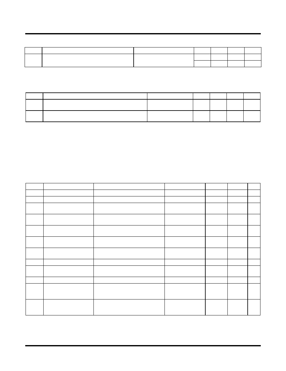
DC and Switching Characteristics
Lattice Semiconductor
LatticeSC/M Family Data Sheet
Power Supply Ramp Rates
Hot Socketing Specifications
1
DC Electrical Characteristics
5
Over Recommended Operating Conditions
Symbol
Parameter
Condition
Min.
Typ.
Max
Units
tRAMP
Power supply ramp rates for all power supplies
Over process, voltage,
temperature
3.45
—
mV/s
——
75
ms
1. See the Power-up and Power-Down requirements section for more details on power sequencing.
2. From 0.5V to minimum operating voltage.
Symbol
Parameter
Condition
Min.
Typ.
Max
Units
IDK
Programmable and dedicated Input or I/O leakage
current
2, 3, 4, 5, 6
0 <= VIN <= VIH (MAX)
—
±1500
A
IHDIN
SERDES average input current when device powered
down and inputs driven
7
——
4
mA
1. See Hot Socket power up/down information in Chapter 2 of this document.
2. Assumes monotonic rise/fall rates for all power supplies.
3. Sensitive to power supply sequencing as described in hot socketing section.
4. Assumes power supplies are between 0 and maximum recommended operations conditions.
5. IDK is additive to IPU, IPD or IBH.
6. Represents DC conditions. For the first 20ns after hot insertion, current specification is 8 mA.
7. Assumes that the device is powered down with all supplies grounded, both P and N inputs driven by a CML driver with maximum allowed
VDDOB of 1.575V, 8b/10b data and internal AC coupling.
Symbol
Parameter
Condition
Min.
3
Typ.
Max.
Units
IIL, IIH
1
Input or I/O Low leakage
0
V
IN VIH (MAX)
—
10
A
IPU
I/O Active Pull-up Current 0
V
IN 0.7 VCCIO
-30
—
-210
A
IPD
I/O Active Pull-down Cur-
rent
VIL (MAX) VIN VIH (MAX)
30
—
210
A
IBHLS
Bus Hold Low Sustaining
Current
VIN = VIL (MAX)
30
—
A
IBHHS
Bus Hold High Sustaining
Current
VIN = 0.7VCCIO
-30
—
A
IBHLO
Bus Hold Low Overdrive
Current
0
V
IN VIH (MAX)
—
210
A
IBHLH
Bus Hold High Overdrive
Current
0
V
IN VIH (MAX)
—
-210
A
ICL
PCI Low Clamp Current
-3 < VIN -1
-25 + (VIN + 1)/0.015
—
mA
ICH
PCI High Clamp Current
VCC + 4 > VIN VCC + 1
25 + (VIN - VCC -1)/
0.015
——
mA
VBHT
Bus Hold trip Points
0
V
IN VIH (MAX)
VIL (MAX)
—
VIH (MIN)
V
C1
I/O Capacitance
2
VCCIO = 3.3V, 2.5V, 1.8V, 1.5V, 1.2V,
VCC = 1.2V, VCCIP2 = 1.2V,
VCCAUX = 2.5, VIO = 0 to VIH (MAX)
—8
—
pf
C3
2
Dedicated Input
Capacitance
2
VCCIO = 3.3V, 2.5V, 1.8V, 1.5V, 1.2V,
VCC = 1.2V, VCCIP2 = 1.2V,
VCCAUX = 2.5, VIO = 0 to VIH (MAX)
—6
—
pf
1. Input or I/O leakage current is measured with the pin configured as an input or as an I/O with the output driver tri-stated. It is not measured
with the output driver active. Bus maintenance circuits are disabled.
2. TA 25°C, f = 1.0MHz
3. IPU, IPD, IBHLS and IBHHS have minimum values of 15 or -15A if VCCIO is set to 1.2V nominal.
4. This table does not apply to SERDES pins.
5. For programmable I/Os.
相關(guān)PDF資料 |
PDF描述 |
|---|---|
| LFSCM3GA40EP1-5FFN1020I | |
| LFXP2-40E-6FN484I | |
| LFXP2-17E-7F484C | |
| LFXP20E-3FN484C | |
| LFXP20E-5FN484C | |
相關(guān)代理商/技術(shù)參數(shù) |
參數(shù)描述 |
|---|---|
| LFSC3GA15E-6FN900C | 功能描述:FPGA - 現(xiàn)場可編程門陣列 15.2K LUTs 3G SERDES 1.2V -6 Spd RoHS:否 制造商:Altera Corporation 系列:Cyclone V E 柵極數(shù)量: 邏輯塊數(shù)量:943 內(nèi)嵌式塊RAM - EBR:1956 kbit 輸入/輸出端數(shù)量:128 最大工作頻率:800 MHz 工作電源電壓:1.1 V 最大工作溫度:+ 70 C 安裝風(fēng)格:SMD/SMT 封裝 / 箱體:FBGA-256 |
| LFSC3GA15E-6FN900I | 功能描述:FPGA - 現(xiàn)場可編程門陣列 15.2K LUTs 3G SERDES 1.2V -6 Spd I RoHS:否 制造商:Altera Corporation 系列:Cyclone V E 柵極數(shù)量: 邏輯塊數(shù)量:943 內(nèi)嵌式塊RAM - EBR:1956 kbit 輸入/輸出端數(shù)量:128 最大工作頻率:800 MHz 工作電源電壓:1.1 V 最大工作溫度:+ 70 C 安裝風(fēng)格:SMD/SMT 封裝 / 箱體:FBGA-256 |
| LFSC3GA15E-7F256C | 功能描述:FPGA - 現(xiàn)場可編程門陣列 15.2K LUTs 3G SERDES 1.2V -7 Spd RoHS:否 制造商:Altera Corporation 系列:Cyclone V E 柵極數(shù)量: 邏輯塊數(shù)量:943 內(nèi)嵌式塊RAM - EBR:1956 kbit 輸入/輸出端數(shù)量:128 最大工作頻率:800 MHz 工作電源電壓:1.1 V 最大工作溫度:+ 70 C 安裝風(fēng)格:SMD/SMT 封裝 / 箱體:FBGA-256 |
| LFSC3GA15E-7F900C | 功能描述:FPGA - 現(xiàn)場可編程門陣列 15.2K LUTs 3G SERDES 1.2V -7 Spd RoHS:否 制造商:Altera Corporation 系列:Cyclone V E 柵極數(shù)量: 邏輯塊數(shù)量:943 內(nèi)嵌式塊RAM - EBR:1956 kbit 輸入/輸出端數(shù)量:128 最大工作頻率:800 MHz 工作電源電壓:1.1 V 最大工作溫度:+ 70 C 安裝風(fēng)格:SMD/SMT 封裝 / 箱體:FBGA-256 |
| LFSC3GA15E-7FN256C | 功能描述:FPGA - 現(xiàn)場可編程門陣列 15.2K LUTs 3G SERDES 1.2V -7 Spd RoHS:否 制造商:Altera Corporation 系列:Cyclone V E 柵極數(shù)量: 邏輯塊數(shù)量:943 內(nèi)嵌式塊RAM - EBR:1956 kbit 輸入/輸出端數(shù)量:128 最大工作頻率:800 MHz 工作電源電壓:1.1 V 最大工作溫度:+ 70 C 安裝風(fēng)格:SMD/SMT 封裝 / 箱體:FBGA-256 |
發(fā)布緊急采購,3分鐘左右您將得到回復(fù)。