- 您現(xiàn)在的位置:買賣IC網(wǎng) > PDF目錄43903 > LC72134M PLL FREQUENCY SYNTHESIZER, 160 MHz, PDSO24 PDF資料下載
參數(shù)資料
| 型號(hào): | LC72134M |
| 元件分類: | PLL合成/DDS/VCOs |
| 英文描述: | PLL FREQUENCY SYNTHESIZER, 160 MHz, PDSO24 |
| 封裝: | MFP-24 |
| 文件頁數(shù): | 5/27頁 |
| 文件大小: | 463K |
| 代理商: | LC72134M |
第1頁第2頁第3頁第4頁當(dāng)前第5頁第6頁第7頁第8頁第9頁第10頁第11頁第12頁第13頁第14頁第15頁第16頁第17頁第18頁第19頁第20頁第21頁第22頁第23頁第24頁第25頁第26頁第27頁
No. 5814-13/27
LC72134M
Continued from preceding page.
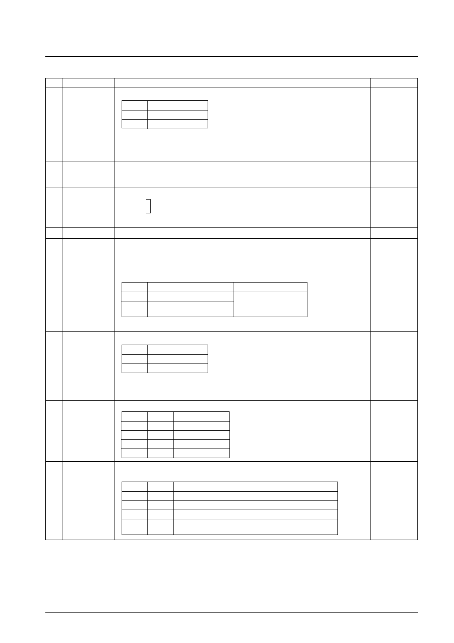
No.
Control block/data
Function
Related data
10
Main charge pump
control data
DLC
Controls the charge pump output (PDa).
* If the circuit deadlocks due to the VCO control voltage (Vtune) being 0 and the VCO being stopped,
applications can get out of the deadlocked state by setting the charge pump output to low and setting
Vtune to VCC. (Deadlock clear circuit)
11
IFS
This data is normally set to 1. Setting this data to 0 sets the circuit to reduced input sensitivity mode, in
which the sensitivity is reduced by about 10 to 30 mV rms.
12
Test data
TEST0 to 2
Test data
TEST0
TEST1
All these bits must be set to 0.
TEST2
All these bits are set to 0 after a power on reset.
13
*
This bit must be set to 0.
14
Sub PLL
programmable
divider data
PS0 to 12
SDVS
Specifies the divisor for the sub PLL programmable divider (FMINb).
The divisor can be set to a value in the range 272 to 8191. Since the internal divide-by-two prescaler is
used, the actual divisor will be twice the set value.
Sets the sub PLL programmable divider operating state.
*: See the “Structure of the Programmable Divider” section for details.
15
Sub PLL charge
pump control data
SDLC
Forcibly controls the charge pump output (PDb).
* If the circuit deadlocks due to the VCO control voltage (Vtune) being 0 and the VCO being stopped,
applications can get out of the deadlocked state by setting the charge pump output to low and setting
Vtune to VCC. (Deadlock clear circuit)
16
Sub PLL reference
divider data
RS0, RS1
Sub PLL reference frequency (fref) selection data
17
Unlocked state
detection output
switching data
ULa, ULb
The unlocked state information output from the DO pin can be selected to be that for either the main PLL
or the sub PLL.
DLC
Charge pump output
0
Normal operation
1
Forced to low
SDLC
Charge pump output
0
Normal operation
1
Forced to low
SDVS
Operating state
Input pin frequency range
1
The FMINb counter operates
0
The FMINb counter is stopped
10 to 160 MHz
(FMINb is pulled down)
RS1
RS0
Reference frequency
0
50
kHz
0
1
25
1
0
12.5
1
15
ULb
ULa
Unlocked state information
0
No unlocked state information is output. The output data, UL is 1.
0
1
Main PLL unlocked state information
1
0
Sub PLL unlocked state information
1
Main PLL plus sub PLL unlocked state information.
(Indicates that either the main or the sub PLL is unlocked.)
相關(guān)PDF資料 |
PDF描述 |
|---|---|
| LC72135M | PLL FREQUENCY SYNTHESIZER, 40 MHz, PDSO20 |
| LC72136NM | PLL FREQUENCY SYNTHESIZER, 40 MHz, PDSO24 |
| LC72140M | PLL FREQUENCY SYNTHESIZER, 160 MHz, PDSO24 |
| LC72140 | PLL FREQUENCY SYNTHESIZER, 160 MHz, PDIP24 |
| LC72146 | PLL FREQUENCY SYNTHESIZER, 40 MHz, PDIP24 |
相關(guān)代理商/技術(shù)參數(shù) |
參數(shù)描述 |
|---|---|
| LC72135M | 制造商:SANYO 制造商全稱:Sanyo Semicon Device 功能描述:PLL Frequency Synthesizer for Electronic Tuning |
| LC72135MA-AE | 功能描述:時(shí)鐘合成器/抖動(dòng)清除器 RoHS:否 制造商:Skyworks Solutions, Inc. 輸出端數(shù)量: 輸出電平: 最大輸出頻率: 輸入電平: 最大輸入頻率:6.1 GHz 電源電壓-最大:3.3 V 電源電壓-最小:2.7 V 封裝 / 箱體:TSSOP-28 封裝:Reel |
| LC72135MA-Q-AE | 制造商:ON Semiconductor 功能描述:PLL FREQUENCY SYNTHESIZER - Tape and Reel 制造商:ON Semiconductor 功能描述:REEL / PLL FREQUENCY SYNTHESIZER |
| LC72135M-Q-TLM-E | 制造商:SANYO Semiconductor Co Ltd 功能描述: |
| LC72136 | 制造商:SANYO 制造商全稱:Sanyo Semicon Device 功能描述:PLL Frequency Synthesizer for Electronic Tuning |
發(fā)布緊急采購,3分鐘左右您將得到回復(fù)。