- 您現(xiàn)在的位置:買賣IC網(wǎng) > PDF目錄358757 > LC662306A (Sanyo Electric Co.,Ltd.) Four-Bit Single-Chip Microcontrollers with 6 KB of On-Chip ROM(4位單片微控制器(帶6K字節(jié)片上ROM)) PDF資料下載
參數(shù)資料
| 型號: | LC662306A |
| 廠商: | Sanyo Electric Co.,Ltd. |
| 英文描述: | Four-Bit Single-Chip Microcontrollers with 6 KB of On-Chip ROM(4位單片微控制器(帶6K字節(jié)片上ROM)) |
| 中文描述: | 四位單芯片6 KB的片上ROM微控制器(4位單片微控制器(帶6清音字節(jié)片上光盤)) |
| 文件頁數(shù): | 14/25頁 |
| 文件大?。?/td> | 158K |
| 代理商: | LC662306A |
Continued from preceding page.
Note: 1. With the output Nch transistor off in shared I/O ports with the open-drain output specifications. These pins cannot be used as input pins if the
CMOS output specifications are selected.
2. With the output Nch transistor off in shared I/O ports with the open-drain output specifications. The rating for the pull-up output specification pins is
stipulated in terms of the output pull-up current IPO. These pins cannot be used as input pins if the CMOS output specifications are selected.
3. With the output Nch transistor off for CMOS output specification pins.
4. With the output Nch transistor off for pull-up output specification pins.
5. With the output Nch transistor off for open-drain output specification pins.
6. Reset state
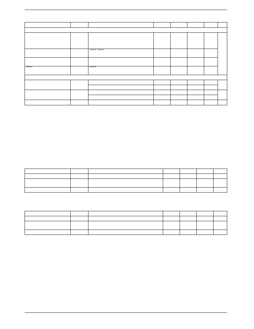
Tone (DTMF) Output Characteristics
DC Characteristics
at Ta = –30 to +70°C, V
SS
= 0 V
1. When the MLOUT enable option is selected (the ML output function can be used)
Note
*
See item 2. below if the MLOUT disable mask option was selected.
2. When the MLOUT disable option is selected (the ML output function cannot be used)
Note
*
See item 1. above if the MLOUT enable mask option was selected.
No. 5483-14/25
LC662304A, 662306A, 662308A, 662312A, 662316A
Parameter
Symbol
Conditions
min
typ
max
Unit
Note
[Pulse conditions]
INT0: Figure 6, conditions under which the INT0
interrupt can be accepted, conditions under
which the timer 0 event counter or pulse width
measurement input can be accepted
INT0 high and low-level
t
IOH
, t
IOL
2
Tcyc
High and low-level pulse widths
for interrupt inputs other than INT0
t
IIH
, t
IIL
INT1, INT2: Figure 6, conditions under which
the corresponding interrupt can be accepted
2
Tcyc
PIN1 high and low-level
pulse widths
t
PINH
, t
PINL
PIN1: Figure 6, conditions under which the
timer 1 event counter input can be accepted
2
Tcyc
RES high and low-level
pulse widths
t
RSH
, t
RSL
RES: Figure 6, conditions under which reset
can be applied.
3
Tcyc
Operating current drain
I
DD OP
V
DD
: 4-MHz ceramic oscillator
V
DD
: 4-MHz external clock
V
DD
: 4-MHz ceramic oscillator
V
DD
: 4-MHz external clock
V
DD
: V
DD
= 1.8 to 5.5 V
4.5
8.0
mA
6
4.5
8.0
mA
Halt mode current drain
I
DDHALT
2.5
5.5
mA
2.5
5.5
mA
Hold mode current drain
I
DDHOLD
0.01
10
μA
Parameter
Symbol
Conditions
min
typ
max
Unit
Tone output voltage (p-p)
V
T1
DT: Dual tones, V
DD
= 3.5 to 5.5 V
*
0.9
1.3
2.0
V
Row/column tone output
voltage ratio
D
BCR1
DT: Dual tones, V
DD
= 3.5 to 5.5 V
*
1.0
2.0
3.0
dB
Tone distortion
THD1
DT: Single tone, V
DD
= 3.5 to 5.5 V
*
2
7
%
Parameter
Symbol
Conditions
min
typ
max
Unit
Tone output voltage (p-p)
V
T1
DT: Dual tones, V
DD
= 3.0 to 5.5 V
*
0.9
1.3
2.0
V
Row/column tone output
voltage ratio
D
BCR1
DT: Dual tones, V
DD
= 3.0 to 5.5 V
*
1.0
2.0
3.0
dB
Tone distortion
THD1
DT: Single tone, V
DD
= 3.0 to 5.5 V
*
2
7
%
相關(guān)PDF資料 |
PDF描述 |
|---|---|
| LC662308A | Four-Bit Single-Chip Microcontroller with 16 KB of On-Chip OTP PROM |
| LC662508A | Four-Bit Single-Chip Microcontrollers with 8, 12, and 16 KB of On-Chip ROM |
| LC66306A | 6K-Byte ROM-Contained Single-Chip 4-Bit Microcontroller for Control-Oriented Application(用于控制導(dǎo)向的單片4位微控制器(帶6K字節(jié)ROM)) |
| LC66354A | Hex Inverters 14-PDIP -40 to 85 |
| LC66354B | Quadruple 2-Input Positive-AND Gates 14-SO -40 to 85 |
相關(guān)代理商/技術(shù)參數(shù) |
參數(shù)描述 |
|---|---|
| LC662308 | 制造商:未知廠家 制造商全稱:未知廠家 功能描述: |
| LC662308A | 制造商:SANYO 制造商全稱:Sanyo Semicon Device 功能描述:Four-Bit Single-Chip Microcontroller with 16 KB of On-Chip OTP PROM |
| LC662312A | 制造商:SANYO 制造商全稱:Sanyo Semicon Device 功能描述:Four-Bit Single-Chip Microcontroller with 16 KB of On-Chip OTP PROM |
| LC662316A | 制造商:SANYO 制造商全稱:Sanyo Semicon Device 功能描述:Four-Bit Single-Chip Microcontroller with 16 KB of On-Chip OTP PROM |
| LC662508A | 制造商:SANYO 制造商全稱:Sanyo Semicon Device 功能描述:Four-Bit Single-Chip Microcontroller with 16 KB of On-Chip OTP PROM |
發(fā)布緊急采購,3分鐘左右您將得到回復(fù)。