- 您現(xiàn)在的位置:買賣IC網(wǎng) > PDF目錄358755 > LC374500ST (Sanyo Electric Co.,Ltd.) Internal Synchronization Silicon Gate 4M (524288-word x 8-bit) mask ROM Pin Compatible with Flash Memory PDF資料下載
參數(shù)資料
| 型號: | LC374500ST |
| 廠商: | Sanyo Electric Co.,Ltd. |
| 英文描述: | Internal Synchronization Silicon Gate 4M (524288-word x 8-bit) mask ROM Pin Compatible with Flash Memory |
| 中文描述: | 內(nèi)同步硅門4米(524288字× 8位)與掩膜ROM閃存引腳兼容 |
| 文件頁數(shù): | 3/4頁 |
| 文件大小: | 46K |
| 代理商: | LC374500ST |
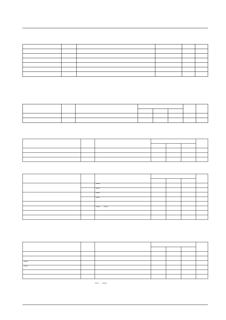
No. 5610-3/4
LC374500ST
Parameter
Symbol
Condition
Rating
Unit
Note
Supply voltage
V
CC
V
IN
V
OUT
Pd max
–0.3 to +7.0
V
1
Input pin voltage
–0.3 to V
CC
+ 0.3
–0.3 to V
CC
+ 0.3
V
1, 2
Output pin voltage
V
1
Allowable power dissipation
Ta = 25°C, reference value for the Sanyo DIP.
1.0
W
1
Operating temperature
Topr
–10 to +70
°C
1
Storage temperature
Tstg
–55 to +125
°C
1
Specifications
Absolute Maximum Ratings
Note: 1. This device may be permanently damaged by stresses in excess of those listed in the maximum ratings. These are stress ratings only, and
functional operation of the device at these conditions or any other conditions beyond those listed in the “DC Allowable Operating Ranges” item is
not implied.
2. The minimum value is –3.0 V for pulse widths of under 30 ns.
Note:
3. These parameters are sampled, and are not measured for every unit.
Note: Values in parentheses are guaranteed at Ta = 25°C.
Note: Values in parentheses are for V
CC
= 4.5 to 5.5 V
*
: t
OD
is defined as the time between the rise of either CE or OE, whichever comes first, and the point when the output goes to the high-impedance
state.
These parameters are sampled, and are not measured for every unit.
Parameter
Symbol
Conditions
Ratings
Unit
Note
min
typ
max
Input pin capacitance
C
IN
C
OUT
V
IN
= 0 V, reference value for the Sanyo DIP.
V
OUT
= 0 V, reference value for the Sanyo DIP.
8
pF
3
Output pin capacitance
10
pF
3
Capacitance Characteristics
at Ta = 25°C, f = 1.0 MHz
Parameter
Symbol
Conditions
Ratings
Unit
min
typ
max
Supply voltage
V
CC
V
IH
V
IL
2.6
5.0
5.5
V
Input high-level voltage
2.2
V
CC
+ 0.3
V
Input low-level voltage
–0.3
+0.6
V
DC Allowable Operating Ranges
at Ta = –10 to +70°C, V
CC
= 2.6 to 5.5 V
Parameter
Symbol
Conditions
Ratings
Unit
min
typ
max
Operating current
I
CCA1
I
CCA2
I
CCS1
I
CCS2
I
LI
I
LO
V
OH
V
OL
CE = 0.2 V, V
I
= V
CC
– 0.2 V/0.2 V
CE = V
IL
, I
O
= 0 mA, V
L
= V
IH
/V
IL
, f = 10 MHz
CE = V
CC
– 0.2 V
CE = V
IH
V
IN
= 0 to V
CC
CE or OE = V
IH
, V
OUT
= 0 to V
CC
I
OH
= –0.5 mA
I
OL
= 0.5 mA
30
μA
55
mA
Standby current
30 (1.0)
μA
1.0 (300)
mA (μA)
Input leakage current
±1.0
μA
Output leakage current
±1.0
μA
Output high-level voltage
0.8 V
CC
V
Output low-level voltage
0.2
V
DC Electrical Characteristics
at Ta = –10 to +70°C, V
CC
= 2.6 to 5.5 V
Parameter
Symbol
Conditions
Ratings
Unit
min
typ
max
Cycle time
t
CYC
t
AA
t
CA
t
OA
t
OH
t
OD
200
ns
Address access time
200 (120)
ns
CE access time
200 (100)
ns
OE access time
80 (40)
ns
Output hold time
20
ns
Output disable time
*
100
ns
AC Characteristics
at Ta = –10 to +70°C, V
CC
= 2.6 to 5.5 V
相關(guān)PDF資料 |
PDF描述 |
|---|---|
| LC374TWN1-25P-A1 | 3-mm Round LED |
| LC374TWN1-25Q-A1 | 3-mm Round LED |
| LC374TWN1-35P-A1 | 3-mm Round LED |
| LC374TWN1-35Q-A1 | 3-mm Round LED |
| LC374TWN1-65P-A1 | 3-mm Round LED |
相關(guān)代理商/技術(shù)參數(shù) |
參數(shù)描述 |
|---|---|
| LC374TWN1-25G-A1 | 制造商:MARKTECH 制造商全稱:Marktech Corporate 功能描述:Ultra Bright White 3mm LED |
| LC374TWN1-25H-A1 | 制造商:MARKTECH 制造商全稱:Marktech Corporate 功能描述:Ultra Bright White 3mm LED |
| LC374TWN1-25P-A1 | 制造商:CREE 制造商全稱:Cree, Inc 功能描述:3-mm Round LED |
| LC374TWN1-25Q-A1 | 制造商:CREE 制造商全稱:Cree, Inc 功能描述:3-mm Round LED |
| LC374TWN1-35P-A1 | 制造商:CREE 制造商全稱:Cree, Inc 功能描述:3-mm Round LED |
發(fā)布緊急采購,3分鐘左右您將得到回復(fù)。