- 您現(xiàn)在的位置:買賣IC網(wǎng) > PDF目錄373149 > KL5KUSB111 (Electronic Theatre Controls, Inc.) USB to HomePNA PDF資料下載
參數(shù)資料
| 型號: | KL5KUSB111 |
| 廠商: | Electronic Theatre Controls, Inc. |
| 英文描述: | USB to HomePNA |
| 中文描述: | USB轉(zhuǎn)電話線網(wǎng)絡(luò) |
| 文件頁數(shù): | 8/8頁 |
| 文件大?。?/td> | 140K |
| 代理商: | KL5KUSB111 |
8
Kawasaki LSI
2570 North First Street
Suite 301
San Jose, CA 95131
Tel: (408) 570-0555
Fax: (408) 570-0567
www.klsi.com
Ver. 2.3
KL5KUSB111
USB to HomePNA
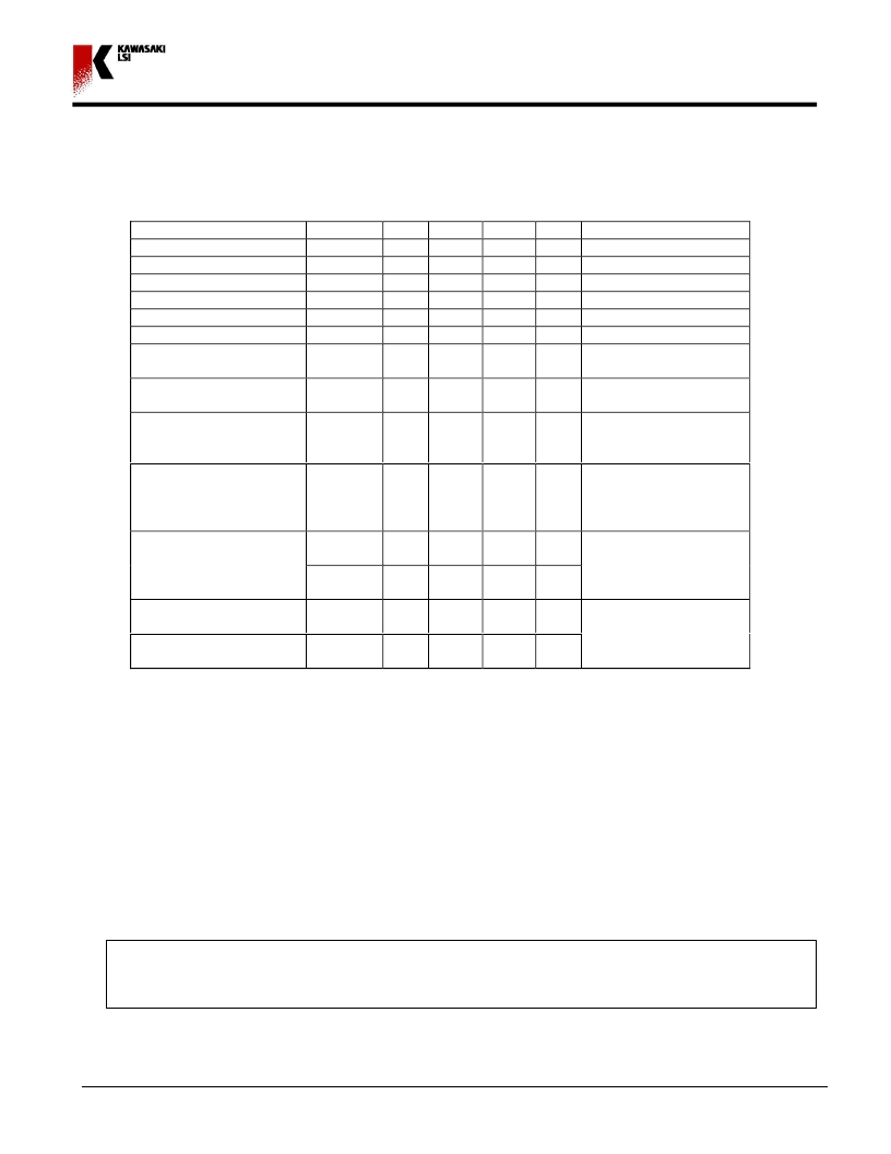
3. I/O Electrical DC Characteristics (Over Recommended Range)
Table 3.1 DC Characteristics (over recommended range)
Symbol
Min
Typ
VIL
–
VIH
2.0
IIL
–10
IIH
–10
Output low voltage
VOL
Output high voltage
VOH
3-state leak current
IOZ
Parameter
Max
0.8
–
10
10
0.4
–
10
Unit
V
V
uA
uA
V
V
uA
Test Conditions
Input low voltage
Input high voltage
Input low current
Input high current
–
–
–
–
–
–
–
VIN = Gnd
VIN = Vdd
IOL = 4mA
IOH = –4mA
VOH = Gnd or VOL =
Vdd
VIN = Gnd or VOH =
Gnd
VIN = Gnd or Vdd
No inputs are cycling.
Outputs open.
Same conditions as
IDDS
except for CLKI input
buffer 48MHz toggling.
Outputs open.
Vdd = Max.
FCLKI = FMAX (
48MHz )
–
2.4
–10
Active pull-up current
IPU
–25
–66
–160
uA
Standby current
IDDS
–
80
100
uA
Suspend current
ISUSP
–
350
450
uA
IDDOP1
(in busy)
IDDOP2
(in idle)
–
80
100
mA
dynamic operating
current
–
40
50
mA
Input capacitance
CIN
–
–
15
pF
Output capacitance
COUT
–
–
15
pF
Fpin=1MHz, VIN =
Gnd.
Vin = 100 mVrms
March 1999
Copyright 1999
Kawasaki LSI
Printed in U.S.A
Kawasaki LSI assumes no responsibility or liability for (1) any errors or inaccuracies contained in the information herein and (2) the use of the
information or a portion thereof in any application, including any claim for (a) copyright or patent infringement or (b) direct, indirect, special or
consequential damages. There are no warranties extended or granted by this document. The information herein is subject to change without notice
form Kawasaki LSI
相關(guān)PDF資料 |
PDF描述 |
|---|---|
| KL5KUSB111_L | USB to HomePNA |
| KL5KUSB116 | USB to Serial |
| KL5KUSB121 | USB to 10/100 Ethernet Controller |
| KL5KUSB121_L | USB to 10/100 Ethernet Controller |
| KL5KUSB200 | USB2.0 Transceiver |
相關(guān)代理商/技術(shù)參數(shù) |
參數(shù)描述 |
|---|---|
| KL5KUSB111_L | 制造商:未知廠家 制造商全稱:未知廠家 功能描述:USB to HomePNA |
| KL5KUSB116 | 制造商:未知廠家 制造商全稱:未知廠家 功能描述:USB to Serial |
| KL5KUSB121 | 制造商:未知廠家 制造商全稱:未知廠家 功能描述:USB to 10/100 Ethernet Controller |
| KL5KUSB121_L | 制造商:未知廠家 制造商全稱:未知廠家 功能描述:USB to 10/100 Ethernet Controller |
| KL5KUSB200 | 制造商:未知廠家 制造商全稱:未知廠家 功能描述:USB2.0 Transceiver |
發(fā)布緊急采購,3分鐘左右您將得到回復(fù)。