- 您現(xiàn)在的位置:買賣IC網(wǎng) > PDF目錄384558 > JANS2N6849U (International Rectifier) HEXFET Transistor(HEXFET MOS場效應管) PDF資料下載
參數(shù)資料
| 型號: | JANS2N6849U |
| 廠商: | International Rectifier |
| 英文描述: | HEXFET Transistor(HEXFET MOS場效應管) |
| 中文描述: | 的HEXFET晶體管(馬鞍山的HEXFET場效應管) |
| 文件頁數(shù): | 2/8頁 |
| 文件大小: | 129K |
| 代理商: | JANS2N6849U |
2
www.irf.com
IRFE9130, JANTX-, JANTXV-, JANS-, 2N6849U Device
Electrical Characteristics
@ Tj = 25°C (Unless Otherwise Specified)
Parameter
Drain-to-Source Breakdown Voltage
Temperature Coefficient of Breakdown
Voltage
Static Drain-to-Source
On-State Resistance
Gate Threshold Voltage
Forward Transconductance
Zero Gate Voltage Drain Current
Min
-100
—
Typ
—
-0.10
Max Units
—
—
Test Conditions
VGS =0 V, ID = -1.0mA
Reference to 25°C, ID = -1.0mA
BVDSS
BVDSS/
TJ
V
V/°C
RDS(on)
—
—
-2.0
1.9
—
—
—
—
—
—
—
—
0.30
0.345
-4.0
—
-25
-250
VGS = -10V, ID = -4.1A
VGS = -10V, ID = -6.5A
VDS = VGS, ID = -250μA
VDS > 15V, IDS = -4.1A
VDS= 0.8 x Max Rating,VGS=0V
VDS = 0.8 x Max Rating
VGS = 0V, TJ = 125°C
VGS = 20 V
VGS = -20V
VGS = -10V, ID = -6.5A
VDS = Max Rating x 0.5
V
VGS(th)
gfs
IDSS
S (
)
IGSS
IGSS
Qg
Qgs
Qgd
td
(on)
tr
td
(off)
tf
LD
Gate-to-Source Leakage Forward
Gate-to-Source Leakage Reverse
Total Gate Charge
Gate-to-Source Charge
Gate-to-Drain (‘Miller’) Charge
Turn-On Delay Time
Rise Time
Turn-Off Delay Time
Fall Time
Internal Drain Inductance
—
—
—
—
—
—
—
—
—
—
—
—
—
—
—
—
—
—
—
1.8
100
-100
35
6.8
23
60
140
140
140
—
nC
VDD = -50V, ID = -6.5A,
RG = 7.5
LS
Internal Source Inductance
—
4.3
—
Ciss
Coss
Crss
Input Capacitance
Output Capacitance
Reverse Transfer Capacitance
—
—
—
790
340
71
—
—
—
VGS = 0V, VDS = -25 V
f = 1.0MHz
pF
Source-Drain Diode Ratings and Characteristics
Parameter
IS
Continuous Source Current (Body Diode)
ISM
Pulse Source Current (Body Diode)
Min Typ
—
—
Max Units
-6.5
-25
Test Conditions
—
—
VSD
trr
QRR
ton
Diode Forward Voltage
Reverse Recovery Time
Reverse Recovery Charge
—
—
—
—
—
—
-4.3
250
3.0
V
ns
μC
T
j
= 25°C, IS = -6.5A, VGS = 0V
Tj = 25°C, IF = -6.5A, di/dt
≤
-100A/
μ
s
VDD
≤
-50V
Forward Turn-On Time
Intrinsic turn-on time is negligible. Turn-on speed is substantially controlled by LS + LD.
A
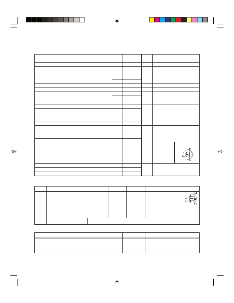
Modified MOSFET symbol
showing the integral reverse
p-n junction rectifier.
nA
nH
ns
Measured fromdrain pad to
die.
Measured fromcenter of
source pad to the end of
source bonding wire.
Modified MOSFET symbol show-
μ
A
Thermal Resistance
Parameter
RthJC
Junction-to-Case
Min Typ Max
—
—
Units
Test Conditions
5.0
K/W
RthJPCB
Junction-to-PC Board
—
—
19
Soldered to a copper clad PC board
Details of notes
through
are on the last page
相關(guān)PDF資料 |
PDF描述 |
|---|---|
| JANTX2N6849 | HEXFET POWER MOSFET(HEXFET 功率MOS場效應管) |
| JANTX2N6851U | HEXFET Transistor(HEXFET MOS場效應管) |
| JANTXV2N6851U | HEXFET Transistor(HEXFET MOS場效應管) |
| JANS2N6851U | HEXFET Transistor(HEXFET MOS場效應管) |
| JANTX2N7221 | HEXFET Transistor(HEXFET 晶體管) |
相關(guān)代理商/技術(shù)參數(shù) |
參數(shù)描述 |
|---|---|
| JANS2N6851 | 制造商:International Rectifier 功能描述:HEXFET, -200V, -4.0A, 0.80 OHM - Rail/Tube |
| JANS2N6851U | 制造商:International Rectifier 功能描述:HEXFET, HI-REL, QPL, SPACE - Bulk |
| JANS2N6987 | 制造商:Microsemi Corporation 功能描述:PNP QUAD TRANSISTOR - Waffle Pack |
| JANS2N6987U | 制造商:Microsemi Corporation 功能描述:Trans GP BJT PNP 60V 0.6A 20-Pin LLCC 制造商:Microsemi Corporation 功能描述:PNP QUAD TRANSISTOR - Bulk 制造商:Microsemi Corporation 功能描述:PNP QUAD TRANSISTOR - Waffle Pack |
| JANS2N6988 | 制造商:Microsemi Corporation 功能描述:PNP QUAD TRANSISTOR - Waffle Pack |
發(fā)布緊急采購,3分鐘左右您將得到回復。