- 您現(xiàn)在的位置:買賣IC網(wǎng) > PDF目錄384537 > ISPLSI1032E-70LTI (Lattice Semiconductor Corporation) High-Density Programmable Logic PDF資料下載
參數(shù)資料
| 型號: | ISPLSI1032E-70LTI |
| 廠商: | Lattice Semiconductor Corporation |
| 英文描述: | High-Density Programmable Logic |
| 中文描述: | 高密度可編程邏輯 |
| 文件頁數(shù): | 2/17頁 |
| 文件大?。?/td> | 301K |
| 代理商: | ISPLSI1032E-70LTI |
2
Specifications
ispLSI and pLSI 1032E
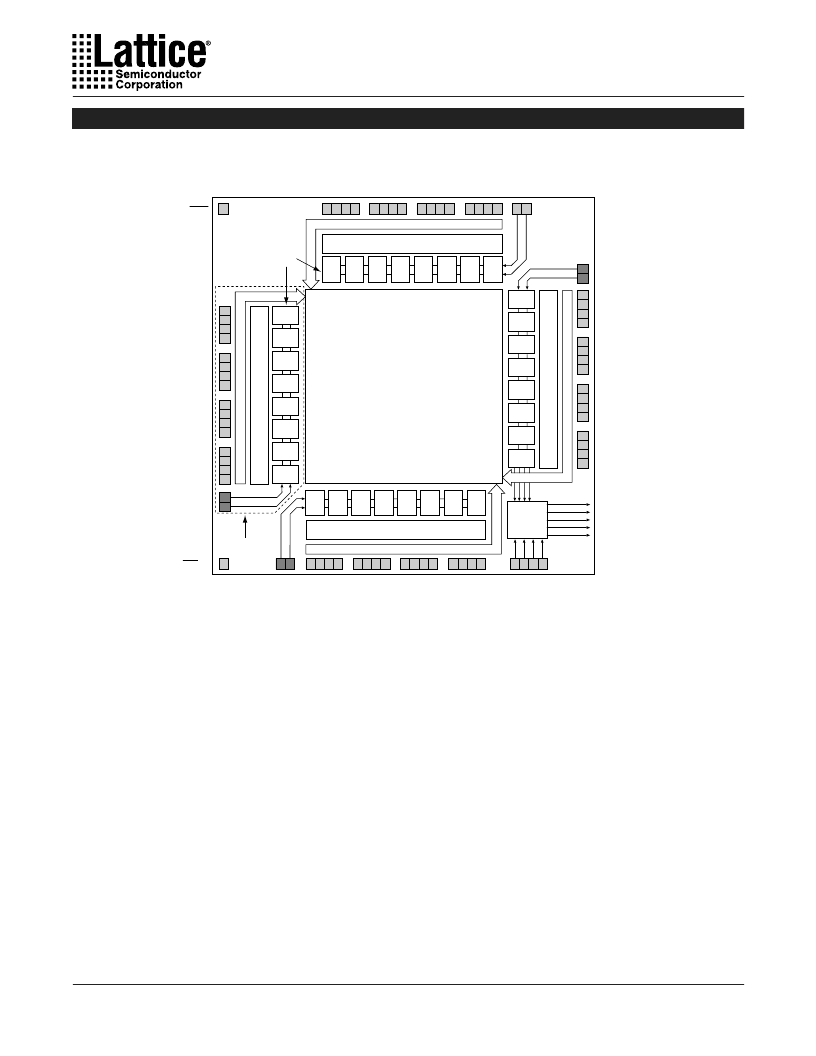
Functional Block Diagram
Figure 1. ispLSI and pLSI 1032E Functional Block Diagram
The devices also have 64 I/O cells, each of which is
directly connected to an I/O pin. Each I/O cell can be
individually programmed to be a combinatorial input,
registered input, latched input, output or bi-directional
I/O pin with 3-state control. The signal levels are TTL
compatible voltages and the output drivers can source 4
mA or sink 8 mA. Each output can be programmed
independently for fast or slow output slew rate to mini-
mize overall output switching noise.
Eight GLBs, 16 I/O cells, two dedicated inputs and one
ORP are connected together to make a Megablock (see
figure 1). The outputs of the eight GLBs are connected to
a set of 16 universal I/O cells by the ORP. Each ispLSI
and pLSI 1032E device contains four Megablocks.
The GRP has, as its inputs, the outputs from all of the
GLBs and all of the inputs from the bi-directional I/O cells.
All of these signals are made available to the inputs of the
GLBs. Delays through the GRP have been equalized to
minimize timing skew.
Clocks in the ispLSI and pLSI 1032E devices are se-
lected using the Clock Distribution Network. Four
dedicated clock pins (Y0, Y1, Y2 and Y3) are brought into
the distribution network, and five clock outputs (CLK 0,
CLK 1, CLK 2, IOCLK 0 and IOCLK 1) are provided to
route clocks to the GLBs and I/O cells. The Clock Distri-
bution Network can also be driven from a special clock
GLB (C0 on the ispLSI and pLSI 1032E devices). The
logic of this GLB allows the user to create an internal
clock from a combination of internal signals within the
device.
I
I
I
I
RESET
Global
Routing
Pool
(GRP)
CLK 0
CLK 1
CLK 2
IOCLK 0
IOCLK 1
Clock
Distribution
Network
C7
C6
C5
C4
C3
C2
C1
C0
A7
A6
A5
A4
A3
A2
A1
A0
Generic
Logic Blocks
(GLBs)
Megablock
O
O
Output Routing Pool (ORP)
Output Routing Pool (ORP)
Input Bus
Input Bus
*ispEN/NC
l
l
*ISP Control Functions for ispLSI 1032E Only
I
I
I
I
I
I
I
I
I
I
I
I
I
I
D7
D6
D5
D4
D3
D2
D1
D0
I
I
I
I
*
*
I
I
I
I
I
I
I
I
I
I
I
I
I/O 35
I/O 34
I/O 33
I/O 32
I/O 0
I/O 1
I/O 2
I/O 3
I/O 12
I/O 13
I/O 14
I/O 15
*SDI/IN 0
*MODE/IN 1
I/O 8
I/O 9
I/O 10
I/O 11
I/O 4
I/O 5
I/O 6
I/O 7
I/O 47
I/O 46
I/O 45
I/O 44
GOE 1/IN 5
GOE 0/IN 4
I/O 43
I/O 42
I/O 41
I/O 40
I/O 39
I/O 38
I/O 37
I/O 36
Y
Y
Y
Y
B0
B1
B2
B3
B4
B5
B6
B7
相關(guān)PDF資料 |
PDF描述 |
|---|---|
| ISP1032E | High-Density Programmable Logic |
| ISPLSI1032E-125LJ | In-System Programmable High Density PLD |
| ISPLSI1032E-125LJ | High-Density Programmable Logic |
| ispLSI1032EA-100LT100 | In-System Programmable High Density PLD |
| ISPLSI1032EA-200LT100 | In-System Programmable High Density PLD |
相關(guān)代理商/技術(shù)參數(shù) |
參數(shù)描述 |
|---|---|
| ISPLSI1032E70LTN | 制造商:LATTICE 制造商全稱:Lattice Semiconductor 功能描述:In-System Programmable High Density PLD |
| ispLSI1032E-70LTN | 功能描述:CPLD - 復(fù)雜可編程邏輯器件 USE ispMACH 4000V RoHS:否 制造商:Lattice 系列: 存儲類型:EEPROM 大電池數(shù)量:128 最大工作頻率:333 MHz 延遲時間:2.7 ns 可編程輸入/輸出端數(shù)量:64 工作電源電壓:3.3 V 最大工作溫度:+ 90 C 最小工作溫度:0 C 封裝 / 箱體:TQFP-100 |
| ISPLSI1032E70LTNI | 制造商:LATTICE 制造商全稱:Lattice Semiconductor 功能描述:In-System Programmable High Density PLD |
| ispLSI1032E-70LTNI | 功能描述:CPLD - 復(fù)雜可編程邏輯器件 USE ispMACH 4000V RoHS:否 制造商:Lattice 系列: 存儲類型:EEPROM 大電池數(shù)量:128 最大工作頻率:333 MHz 延遲時間:2.7 ns 可編程輸入/輸出端數(shù)量:64 工作電源電壓:3.3 V 最大工作溫度:+ 90 C 最小工作溫度:0 C 封裝 / 箱體:TQFP-100 |
| ISPLSI1032E80LJ | 制造商:未知廠家 制造商全稱:未知廠家 功能描述:Electrically-Erasable Complex PLD |
發(fā)布緊急采購,3分鐘左右您將得到回復(fù)。