- 您現(xiàn)在的位置:買賣IC網(wǎng) > PDF目錄384495 > IRFF9220 (International Rectifier) REPETITIVE AVALANCHE AND dv/dt RATED HEXFET剖TRANSISTORS THRU-HOLE (TO-205AF) PDF資料下載
參數(shù)資料
| 型號: | IRFF9220 |
| 廠商: | International Rectifier |
| 英文描述: | REPETITIVE AVALANCHE AND dv/dt RATED HEXFET剖TRANSISTORS THRU-HOLE (TO-205AF) |
| 中文描述: | 重復(fù)性雪崩和DV /受好評的HEXFET剖三極管通孔dt(下至205AF) |
| 文件頁數(shù): | 2/7頁 |
| 文件大小: | 327K |
| 代理商: | IRFF9220 |
4-108
Absolute Maximum Ratings
T
C
= 25
o
C, Unless Otherwise Specified
IRFF9220
-200
-200
-2.5
-10
±
20
20
0.16
290
-55 to 150
UNITS
V
V
A
A
V
W
W/
o
C
mJ
o
C
Drain to Source Breakdown Voltage (Note 1) . . . . . . . . . . . . . . . . . . . . . . . . . . . . . . . . . . . . . . .V
DS
Drain to Gate Voltage (R
GS
= 20k
)
(Note 1) . . . . . . . . . . . . . . . . . . . . . . . . . . . . . . . . . . . . . V
DGR
Continuous Drain Current . . . . . . . . . . . . . . . . . . . . . . . . . . . . . . . . . . . . . . . . . . . . . . . . . . . . . . . I
D
Pulsed Drain Current (Note 3) . . . . . . . . . . . . . . . . . . . . . . . . . . . . . . . . . . . . . . . . . . . . . . . . . . . I
DM
Gate to Source Voltage . . . . . . . . . . . . . . . . . . . . . . . . . . . . . . . . . . . . . . . . . . . . . . . . . . . . . . . .V
GS
Maximum Power Dissipation . . . . . . . . . . . . . . . . . . . . . . . . . . . . . . . . . . . . . . . . . . . . . . . . . . . . .P
D
Linear Derating Factor . . . . . . . . . . . . . . . . . . . . . . . . . . . . . . . . . . . . . . . . . . . . . . . . . . . . . . . . . . . .
Single Pulse Avalanche Energy Rating (Note 4). . . . . . . . . . . . . . . . . . . . . . . . . . . . . . . . . . . . . . .E
AS
Operating and Storage Temperature . . . . . . . . . . . . . . . . . . . . . . . . . . . . . . . . . . . . . . . . . .T
J,
T
STG
Maximum Temperature for Soldering
Leads at 0.063in (1.6mm) from Case for 10s. . . . . . . . . . . . . . . . . . . . . . . . . . . . . . . . . . . . . . . T
L
CAUTION: Stresses above those listed in “Absolute Maximum Ratings” may cause permanent damage to the device. This is a stress only rating and operation of the
device at these or any other conditions above those indicated in the operational sections of this specification is not implied.
300
o
C
NOTE:
1. T
J
= 25
o
C to 125
o
C.
Electrical Specifications
T
C
= 25
o
C, Unless Otherwise Specified
PARAMETER
SYMBOL
TEST CONDITIONS
MIN
TYP
MAX
UNITS
Drain to Source Breakdown Voltage
BV
DSS
V
GS(TH)
I
DSS
I
D
= -250
μ
A, V
GS
= 0V, (Figure 10)
V
GS
= V
DS
, I
D
= -250
μ
A
V
DS
= Rated BV
DSS
, V
GS
= 0V
V
DS
= 0.8 x Rated BV
DSS
, V
GS
= 0V, T
C
= 125
o
C
V
DS
> I
D(ON)
x r
DS(ON)MAX
, V
GS
= -10V
V
GS
=
±
20V
I
D
= 1.5A, V
GS
= -10V, (Figures 8, 9)
V
DS
> I
D(ON)
x r
DS(ON)MAX
, I
D
= 1.5A,
(Figure 12)
-200
-
-
V
Gate Threshold Voltage
-2
-
-4
V
Zero Gate Voltage Drain Current
-
-
-25
μ
A
-
-
-250
μ
A
On-State Drain Current (Note 2)
I
D(ON)
I
GSS
r
DS(ON)
g
fs
-2.5
-
-
A
Gate to Source Leakage Current
-
-
±
100
nA
Drain to Source On Resistance (Note 2)
-
1.0
1.5
Forward Transconductance (Note 2)
1
1.8
-
S
Turn-On Delay Time
t
d(ON)
t
r
t
d(OFF)
t
f
V
DD
= 0.5 x Rated BV
DSS
, I
D
= -2.5A, R
GS
= 9.1
,
R
L
= 38.5
for BV
DSS
= -200V
R
L
= 28.5
for BV
DSS
= -150V
(Figures 17, 18) MOSFET Switching Times are
Essentially Independent of Operating
Temperature
-
15
40
ns
Rise Time
-
25
50
ns
Turn-Off Delay Time
-
80
120
ns
Fall Time
-
50
75
ns
Total Gate Charge
(Gate to Source + Gate to Drain)
Q
g(TOT)
V
GS
= -10V, I
D
= -2.5A, V
DS
= 0.8 x Rated BV
DSS
I
G(REF)
= -1.5mA, (Figures 14, 19, 20)
Gate Charge is Essentially Independent of
Operating Temperature
-
16
22
nC
Gate to Source Charge
Q
gs
Q
gd
C
ISS
C
OSS
C
RSS
L
D
-
9
-
nC
Gate to Drain “Miller” Charge
-
7
-
nC
Input Capacitance
V
DS
= -25V, V
GS
= 0V, f = 1MHz, (Figure 11)
-
350
-
pF
Output Capacitance
-
100
-
pF
Reverse Transfer Capacitance
-
30
-
pF
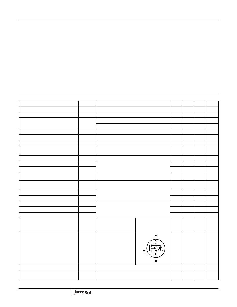
Internal Drain Inductance
Measured From the Drain
Lead, 5mm (0.2in) From
Header To Center of Die
Modified MOSFET
Symbol Showing the In-
ternal Devices
Inductances
-
5.0
-
nH
Internal Source Inductance
L
S
MeasuredFromtheSource
Lead, 5mm (0.2in) From
Header to Source Bonding
Pad
-
15
-
nH
Thermal Resistance Junction to Case
R
θ
JC
R
θ
JA
-
-
6.25
o
C/W
o
C/W
Thermal Resistance
Junction to Ambient
Typical Socket Mount
-
-
175
L
S
L
D
G
D
S
IRFF9220
相關(guān)PDF資料 |
PDF描述 |
|---|---|
| IRFF9230 | -4.0A, -200V, 0.800 Ohm, P-Channel Power MOSFET |
| IRFF9230 | HEXFET TRANSISTORS THRU-HOLE (TO-205AF) |
| IRFG110 | POWER MOSFET THRU-HOLE (MO-036AB) |
| IRFG5110 | 100V, Combination 2N-2P-CHANNEL |
| IRFG6110 | POWER MOSFET THRU-HOLE (MO-036AB) |
相關(guān)代理商/技術(shù)參數(shù) |
參數(shù)描述 |
|---|---|
| IRFF9221 | 制造商:Rochester Electronics LLC 功能描述:- Bulk |
| IRFF9222 | 制造商:Rochester Electronics LLC 功能描述:- Bulk |
| IRFF9223 | 制造商:未知廠家 制造商全稱:未知廠家 功能描述:TRANSISTOR | MOSFET | P-CHANNEL | 150V V(BR)DSS | 2A I(D) | TO-205AA |
| IRFF9230 | 制造商:International Rectifier 功能描述:Trans MOSFET P-CH 200V 4A 3-Pin TO-39 制造商:International Rectifier 功能描述:TRANS MOSFET P-CH 200V 4A 3PIN TO-39 - Bulk 制造商:International Rectifier 功能描述:200V SINGLE P-CHANNEL HI-REL MOSFET 制造商:Rochester Electronics LLC 功能描述:- Bulk 制造商:International Rectifier 功能描述:P CH MOSFET -200V 4A TO-205AF 制造商:International Rectifier 功能描述:P CH MOSFET, -200V, 4A, TO-205AF 制造商:International Rectifier 功能描述:P CH MOSFET, -200V, 4A, TO-205AF; Transistor Polarity:P Channel; Continuous Drain Current Id:-4A; Drain Source Voltage Vds:-200V; On Resistance Rds(on):800mohm; Rds(on) Test Voltage Vgs:-10V; Threshold Voltage Vgs Typ:-4V ;RoHS Compliant: No |
| IRFF9231 | 制造商:International Rectifier 功能描述: |
發(fā)布緊急采購,3分鐘左右您將得到回復(fù)。