- 您現(xiàn)在的位置:買(mǎi)賣(mài)IC網(wǎng) > PDF目錄299200 > IDT7005L55PF (INTEGRATED DEVICE TECHNOLOGY INC) Dual, Ultra Low Cost, RRIO CMOS Amplifier PDF資料下載
參數(shù)資料
| 型號(hào): | IDT7005L55PF |
| 廠商: | INTEGRATED DEVICE TECHNOLOGY INC |
| 元件分類(lèi): | SRAM |
| 英文描述: | Dual, Ultra Low Cost, RRIO CMOS Amplifier |
| 中文描述: | 8K X 8 DUAL-PORT SRAM, 55 ns, PQFP64 |
| 封裝: | 14 X 14 MM, 1.40 MM HEIGHT, TQFP-64 |
| 文件頁(yè)數(shù): | 17/20頁(yè) |
| 文件大?。?/td> | 189K |
| 代理商: | IDT7005L55PF |
第1頁(yè)第2頁(yè)第3頁(yè)第4頁(yè)第5頁(yè)第6頁(yè)第7頁(yè)第8頁(yè)第9頁(yè)第10頁(yè)第11頁(yè)第12頁(yè)第13頁(yè)第14頁(yè)第15頁(yè)第16頁(yè)當(dāng)前第17頁(yè)第18頁(yè)第19頁(yè)第20頁(yè)
6.42
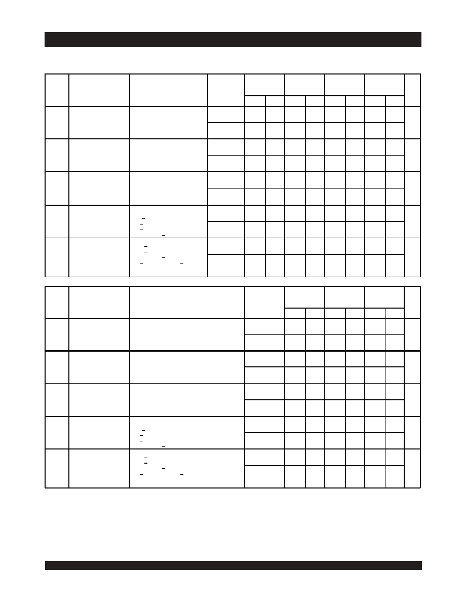
IDT7005S/L
High-Speed 8K x 8 Dual-Port Static RAM
Military, Industrial and Commercial Temperature Ranges
6
DC Electrical Characteristics Over the Operating
Temperature and Supply Voltage Range(1,6) (VCC = 5.0V ± 10%)
NOTES:
1.
'X' in part number indicates power rating (S or L)
2.
VCC = 5V, TA = +25°C and are not production tested. ICC DC = 120mA (typ)
3.
At f = fMAX
, address and I/O'S are cycling at the maximum frequency read cycle of 1/tRC, and using “AC Test Conditions” of input levels of GND to 3V.
4.
f = 0 means no address or control lines change.
5.
Port "A" may be either left or right port. Port "B" is the port opposite port "A".
6.
Industrial temperature: for other speeds, packages and powers contact your sales office.
7005X15
Com'l Only
7005X17
Com'l Only
7005X20
Com'l &
Military
7005X25
Com'l &
Military
Symbol
Parameter
Test Condition
Version
Typ.(2)
Max.
Typ.(2)
Max.
Typ.(2)
Max.
Typ.(2)
Max.
Unit
ICC
Dynamic Operating Current
(Both Ports Active)
CE = VIL, Outputs Disabled
SEM = VIH
f = fMAX
(3)
COM'L
S
L
170
160
310
260
170
160
310
260
160
150
290
240
155
145
265
220
mA
MIL &
IND
S
L
____
160
150
370
320
155
145
340
280
ISB1
Standby Current
(Both Ports - TTL
Level Inputs)
CEL = CER = VIH
SEMR = SEML = VIH
f = fMAX(3)
COM'L
S
L
20
10
60
20
10
60
50
20
10
60
50
16
10
60
50
mA
MIL &
IND
S
L
____
20
10
90
70
16
10
80
65
ISB2
Standby Current
(One Port - TTL
Level Inputs)
CE"A" = VIL and CE"B" = VIH(5)
Active Port Outputs Disabled
f=fMAX
(3)
SEMR = SEML = VIH
COM'L
S
L
105
95
190
160
105
95
190
160
95
85
180
150
90
80
170
140
mA
MIL &
IND
S
L
____
95
85
240
210
90
80
215
180
ISB3
Full Standby Current (Both
Ports - All CMOS Level
Inputs)
Both Ports
CEL and
CER > VCC - 0.2V
VIN > VCC - 0.2V or
VIN < 0.2V, f = 0(4)
SEMR = SEML > VCC - 0.2V
COM'L
S
L
1.0
0.2
15
5
1.0
0.2
15
5
1.0
0.2
15
5
1.0
0.2
15
5
mA
MIL &
IND
S
L
____
1.0
0.2
30
10
1.0
0.2
30
10
ISB4
Full Standby Current
(One Port - All
CMOS Level Inputs)
CE"A" < 0.2V and
CE"B" > VCC - 0.2V(5)
SEMR = SEML > VCC - 0.2V
VIN > VCC - 0.2V or VIN < 0.2V
Active Port Outputs Disabled
f = fMAX
(3)
COM'L
S
L
100
90
170
140
100
90
170
140
90
80
155
130
85
75
145
120
mA
MIL &
IND
S
L
____
90
80
225
200
85
75
200
170
2738 tbl 10
7005X35
Com'l, Ind
& Military
7005X55
Com'l, Ind
& Military
7005X70
Military
Only
Symbol
Parameter
Test Condition
Version
Typ.(2)
Max.
Typ.(2)
Max.
Typ.(2)
Max.
Unit
ICC
Dynamic Operating
Current
(Both Ports Active)
CE = VIL, Outputs Disabled
SEM = VIH
f = fMAX
(3)
COM'L
S
L
150
140
250
210
150
140
250
210
____
mA
MIL &
IND
S
L
150
140
300
250
150
140
300
250
140
130
300
250
ISB1
Standby Current
(Both Ports - TTL
Level Inputs)
CEL = CER = VIH
SEMR = SEML = VIH
f = fMAX(3)
COM'L
S
L
13
10
60
50
13
10
60
50
____
mA
MIL &
IND
S
L
13
10
80
65
13
10
80
65
10
8
80
65
ISB2
Standby Current
(One Port - TTL
Level Inputs)
CE"A" = VIL and CE"B" = VIH(5)
Active Port Outputs Disabled
f=fMAX(3)
SEMR = SEML = VIH
COM'L
S
L
85
75
155
130
85
75
155
130
____
mA
MIL &
IND
S
L
85
75
190
160
85
75
190
160
80
70
190
160
ISB3
Full Standby Current
(Both Ports - All
CMOS Level Inputs)
Both Ports
CEL and
CER > VCC - 0.2V
VIN > VCC - 0.2V or
VIN < 0.2V, f = 0
(4)
SEMR = SEML > VCC - 0.2V
COM'L
S
L
1.0
0.2
15
5
1.0
0.2
15
5
____
mA
MIL &
IND
S
L
1.0
0.2
30
10
1.0
0.2
30
10
1.0
0.2
30
10
ISB4
Full Standby Current
(One Port - All
CMOS Level Inputs)
CE"A" < 0.2V and
CE"B" > VCC - 0.2V(5)
SEMR = SEML > VCC - 0.2V
VIN > VCC - 0.2V or VIN < 0.2V
Active Port Outputs Disabled
f = fMAX(3)
COM'L
S
L
80
70
135
110
80
70
135
110
____
mA
MIL &
IND
S
L
80
70
175
150
80
70
175
150
75
65
175
150
2738 tbl 11
相關(guān)PDF資料 |
PDF描述 |
|---|---|
| IDT7005L55PFB | HIGH-SPEED 8K x 8 DUAL-PORT STATIC RAM |
| IDT7005S | HIGH-SPEED 8K x 8 DUAL-PORT STATIC RAM |
| IDT7034L20PF8 | 4K X 18 DUAL-PORT SRAM, 20 ns, PQFP100 |
| IDT709199L12PFG | 128K X 9 DUAL-PORT SRAM, 25 ns, PQFP100 |
| IDT70V34TS20PFI | 4K X 18 DUAL-PORT SRAM, 20 ns, PQFP100 |
相關(guān)代理商/技術(shù)參數(shù) |
參數(shù)描述 |
|---|---|
| IDT7005L55PF8 | 功能描述:IC SRAM 64KBIT 55NS 64TQFP RoHS:否 類(lèi)別:集成電路 (IC) >> 存儲(chǔ)器 系列:- 標(biāo)準(zhǔn)包裝:72 系列:- 格式 - 存儲(chǔ)器:RAM 存儲(chǔ)器類(lèi)型:SRAM - 同步 存儲(chǔ)容量:9M(256K x 36) 速度:75ns 接口:并聯(lián) 電源電壓:3.135 V ~ 3.465 V 工作溫度:-40°C ~ 85°C 封裝/外殼:100-LQFP 供應(yīng)商設(shè)備封裝:100-TQFP(14x14) 包裝:托盤(pán) 其它名稱(chēng):71V67703S75PFGI |
| IDT7005L55PFB | 制造商:IDT 制造商全稱(chēng):Integrated Device Technology 功能描述:HIGH-SPEED 8K x 8 DUAL-PORT STATIC RAM |
| IDT7005L55XL | 制造商:未知廠家 制造商全稱(chēng):未知廠家 功能描述:x8 Dual-Port SRAM |
| IDT7005L55XLB | 制造商:未知廠家 制造商全稱(chēng):未知廠家 功能描述:x8 Dual-Port SRAM |
| IDT7005L70F | 制造商:IDT 制造商全稱(chēng):Integrated Device Technology 功能描述:HIGH-SPEED 8K x 8 DUAL-PORT STATIC RAM |
發(fā)布緊急采購(gòu),3分鐘左右您將得到回復(fù)。