- 您現(xiàn)在的位置:買賣IC網(wǎng) > PDF目錄357919 > ICS507M-02I Circular Connector; MIL SPEC:MIL-C-5015 E/F/R; Body Material:Aluminum Alloy; Series:SG3102; Number of Contacts:19; Connector Shell Size:24; Connecting Termination:Solder; Circular Shell Style:Box Mount Receptacle PDF資料下載
參數(shù)資料
| 型號(hào): | ICS507M-02I |
| 元件分類: | 圓形連接器 |
| 英文描述: | Circular Connector; MIL SPEC:MIL-C-5015 E/F/R; Body Material:Aluminum Alloy; Series:SG3102; Number of Contacts:19; Connector Shell Size:24; Connecting Termination:Solder; Circular Shell Style:Box Mount Receptacle |
| 中文描述: | PECL的時(shí)鐘合成器 |
| 文件頁(yè)數(shù): | 3/5頁(yè) |
| 文件大小: | 49K |
| 代理商: | ICS507M-02I |
ICS507-01/02
PECL Clock Synthesizer
MDS 507 C
Integrated Circuit Systems, Inc. 525 Race Street San Jose CA 95126 (408)295-9800tel www.icst.com
3
Revision 042600
Printed 11/13/00
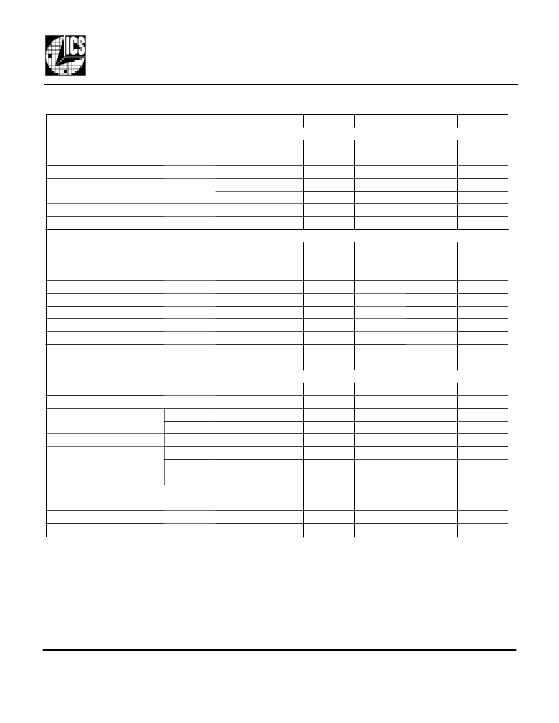
Parameter
ABSOLUTE MAXIMUM RATINGS (stresses be ond these can permanentl damage the device)
Supply Voltage, VDD
Referenced to GND
Inputs
Referenced to GND
Clock Output
Referenced to GND
Ambient Operating Temperature
ICS507M-0x
ICS507M-0xI
Soldering Temperature
Max of 20 seconds
Storage temperature
DC CHARACTERISTICS (VDD = 5.0 V unless otherwise noted)
Operating Voltage, VDD
Input High Voltage, VIH
ICLK only
Input Low Voltage, VIL
ICLK only
Input High Voltage, VIH
S0, S1
Input Low Voltage, VIL
S0, S1
Output High Voltage, VOH
Note 2
Output Low Voltage, VOL
Note 2
IDD Operating Suppl Current, note 3
No Load, 155.52MHz
Internal Cr stal Capacitance, X1 and X2
Pins 1, 8
Input Capacitance
S0, S1
AC CHARACTERISTICS (VDD = 5.0 V unless otherwise noted)
Input Crystal Frequency
Input Clock Frequency
Output Frequency, ICS507-01
0 to 70°C VDD = 5.0 V
0 to 70°C VDD = 3.3 V
Output Frequency, ICS507-01I
-40 to 85°C VDD = 3.3 V or 5.0 V
Output Frequency, ICS507-02I
0 to 70°C VDD = 5.0 V
0 to 70°C VDD = 3.3 V
-40 to 85°C VDD = 3.3 V or 5.0 V
Output Clock Duty Cycle
PLL Bandwidth
Absolute Clock Period Jitter
Deviation from mean
One Sigma Clock Period Jitter
Conditions
Minimum
Typical
Maximum
Units
7
V
V
V
°C
°C
°C
°C
-0.5
-0.5
0
-40
VDD+0.5
VDD+0.5
70
85
260
150
-65
3.0
5.5
V
V
V
V
V
V
V
VDD/2 + 1
VDD/2
VDD/2
VDD/2-1
VDD-0.5
VDD+0.5
VDD-1.2
VDD-2.0
67
26
4
mA
pF
pF
5
5
10
10
10
125
125
125
49
10
27
52
200
156
125
200
200
160
51
MH z
MH z
MH z
MH z
MH z
MH z
MH z
MH z
%
kHz
ps
ps
±75
20
Electrical Specifications
Notes:
1) All typical values are at 5.0 V and 25°C unless otherwise noted.
2) VOH and VOL can be set by the external resistor values on the PECL outputs.
3) IDD includes the current through the external resistors, which can be modified.
4) The phase relationship between input and output can change at power up. For a fixed phase relationship, see one of the
ICS zero delay buffers.
相關(guān)PDF資料 |
PDF描述 |
|---|---|
| ICS507M-02IT | ER 7C 7#8 PIN RECP |
| ICS507-01 | POWER QUICC |
| ICS507-01-DPK | PECL Clock Synthesizer |
| ICS507-01-DSW | PECL Clock Synthesizer |
| ICS507-01-DWF | PECL Clock Synthesizer |
相關(guān)代理商/技術(shù)參數(shù) |
參數(shù)描述 |
|---|---|
| ICS507M-02IT | 制造商:ICS 制造商全稱:ICS 功能描述:PECL Clock Synthesizer |
| ICS507-XX | 制造商:ICS 制造商全稱:ICS 功能描述:PECL Clock Synthesizer |
| ICS508 | 制造商:ICS 制造商全稱:ICS 功能描述:PECL to CMOS Converter |
| ICS508-DPK | 制造商:ICS 制造商全稱:ICS 功能描述:PECL to CMOS Converter |
| ICS508-DWF | 制造商:ICS 制造商全稱:ICS 功能描述:PECL to CMOS Converter |
發(fā)布緊急采購(gòu),3分鐘左右您將得到回復(fù)。