- 您現(xiàn)在的位置:買賣IC網(wǎng) > PDF目錄385436 > HYS72T256020HU-3.7-A (QIMONDA AG) 240-Pin Unbuffered DDR2 SDRAM Modules PDF資料下載
參數(shù)資料
| 型號: | HYS72T256020HU-3.7-A |
| 廠商: | QIMONDA AG |
| 元件分類: | DRAM |
| 英文描述: | 240-Pin Unbuffered DDR2 SDRAM Modules |
| 中文描述: | 256M X 72 DDR DRAM MODULE, 0.5 ns, DMA240 |
| 封裝: | GREEN, DIMM-240 |
| 文件頁數(shù): | 24/61頁 |
| 文件大小: | 1365K |
| 代理商: | HYS72T256020HU-3.7-A |
第1頁第2頁第3頁第4頁第5頁第6頁第7頁第8頁第9頁第10頁第11頁第12頁第13頁第14頁第15頁第16頁第17頁第18頁第19頁第20頁第21頁第22頁第23頁當前第24頁第25頁第26頁第27頁第28頁第29頁第30頁第31頁第32頁第33頁第34頁第35頁第36頁第37頁第38頁第39頁第40頁第41頁第42頁第43頁第44頁第45頁第46頁第47頁第48頁第49頁第50頁第51頁第52頁第53頁第54頁第55頁第56頁第57頁第58頁第59頁第60頁第61頁

Internet Data Sheet
Rev. 1.32, 2006-09
03062006-5RK8-1X8J
24
HYS[64/72]T256xxxHU–[3/…/5]–A
Unbuffered DDR2 SDRAM Modules
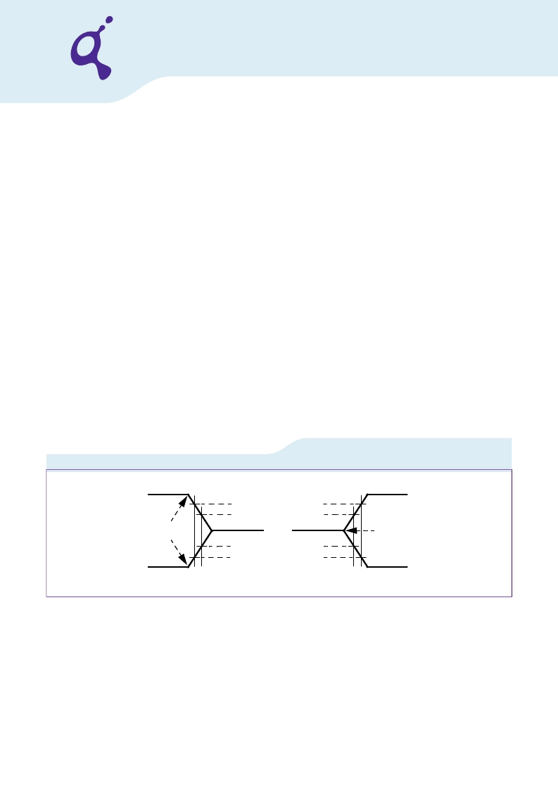
FIGURE 3
Method for calculating transitions and endpoint
26) When the device is operated with input clock jitter, this parameter needs to be derated by the actual
t
JIT.PER
of the input clock. (output
deratings are relative to the SDRAM input clock.) For example, if the measured jitter into a DDR2–667 SDRAM has
t
JIT.PER.MIN
= – 72 ps
and
t
JIT.PER.MAX
= + 93 ps, then
t
=
t
+
t
= 0.9 x
t
– 72 ps = + 2178 ps and
t
RPRE.MAX(DERATED)
=
t
RPRE.MAX
+
t
JIT.PER.MAX
t
CK.AVG
+ 93 ps = + 2843 ps. (Caution on the MIN/MAX usage!).
27) When the device is operated with input clock jitter, this parameter needs to be derated by the actual
t
of the input clock. (output
deratings are relative to the SDRAM input clock.) For example, if the measured jitter into a DDR2–667 SDRAM has
t
JIT.DUTY.MIN
= – 72 ps
and
t
JIT.DUTY.MAX
= + 93 ps, then
t
=
t
+
t
= 0.4 x
t
– 72 ps = + 928 ps and
t
RPST.MAX(DERATED)
=
t
RPST.MAX
+
t
JIT.DUTY.MAX
t
CK.AVG
+ 93 ps = + 1592 ps. (Caution on the MIN/MAX usage!).
28) For these parameters, the DDR2 SDRAM device is characterized and verified to support
t
= RU{
t
PARAM
/
t
CK.AVG
}, which is in clock
cycles, assuming all input clock jitter specifications are satisfied. For example, the device will support
t
nRP
t
}, which is in
clock cycles, if all input clock jitter specifications are met. This means: For DDR2–667 5–5–5, of which
t
RP
= 15 ns, the device will support
t
= RU{
t
/
t
} = 5, i.e. as long as the input clock jitter specifications are met, Precharge command at Tm and Active command at
Tm + 5 is valid even if (Tm + 5 - Tm) is less than 15 ns due to input clock jitter.
29) DAL = WR + RU{
t
(ns) /
t
(ns)}, where RU stands for round up. WR refers to the tWR parameter stored in the MRS. For
t
, if the result
of the division is not already an integer, round up to the next highest integer.
t
refers to the application clock period. Example: For
DDR2–533 at
t
CK
= 3.75 ns with
t
WR
programmed to 4 clocks.
t
DAL
= 4 + (15 ns / 3.75 ns) clocks = 4 + (4) clocks = 8 clocks.
30)
t
DAL.nCK
= WR [nCK] +
t
nRP.nCK
= WR + RU{
t
RP
[ps] /
t
CK.AVG
[ps] }, where WR is the value programmed in the EMR.
31)
t
WTR
is at lease two clocks (2 x
t
CK
) independent of operation frequency.
32)
t
CKE.MIN
of 3 clocks means CKE must be registered on three consecutive positive clock edges. CKE must remain at the valid input level the
entire time it takes to achieve the 3 clocks of registration. Thus, after any CKE transition, CKE may not transition from its valid level during
the time period of
t
IS
+ 2 x
t
CK
+
t
IH
.
33) ODT turn on time min is when the device leaves high impedance and ODT resistance begins to turn on. ODT turn on time max is when
the ODT resistance is fully on. Both are measured from
t
AOND
.
34) ODT turn off time min is when the device starts to turn off ODT resistance. ODT turn off time max is when the bus is in high impedance.
Both are measured from
t
AOFD
.
35) When the device is operated with input clock jitter, this parameter needs to be derated by {–
t
–
t
} and {–
t
–
t
} of the actual input clock. (output deratings are relative to the SDRAM input clock.) For example, if the measured jitter
into a DDR2–667 SDRAM has
t
ERR(6-10PER).MIN
= – 272 ps,
t
ERR(6- 10PER).MAX
= + 293 ps,
t
JIT.DUTY.MIN
= – 106 ps and
t
JIT.DUTY.MAX
= + 94 ps,
then
t
AOF.MIN(DERATED)
=
t
AOF.MIN
+ {–
–
t
} = – 450 ps + {– 94 ps – 293 ps} = – 837 ps and
t
AOF.MAX(DERATED)
=
t
AOF.MAX
+ {–
t
JIT.DUTY.MIN
ERR(6-10PER).MIN
} = 1050 ps + {106 ps + 272 ps} = + 1428 ps. (Caution on the MIN/MAX usage!)
tHZ
tRPST
end point
T1 T2
VOH - x mV
VOH - 2x mV
VOL + 2x mV
VOL + x mV
tLZ
tRPRE
begin point
T2
T1
VTT + 2x mV
VTT + x mV
VTT - x mV
VTT - 2x mV
tLZ,tRPRE
begin point
= 2*T1-T2
tHZ,tRPST
end point
= 2*T1-T2
相關PDF資料 |
PDF描述 |
|---|---|
| HYS72T256020HU-3-A | 240-Pin Unbuffered DDR2 SDRAM Modules |
| HYS72T256020HU-5-A | 240-Pin Unbuffered DDR2 SDRAM Modules |
| HYS72T256023 | 240-Pin Registered DDR2 SDRAM Modules |
| HYS72T256023HR | 240-Pin Registered DDR2 SDRAM Modules |
| HYS72T256023HR-5-A | 240-Pin Registered DDR2 SDRAM Modules |
相關代理商/技術參數(shù) |
參數(shù)描述 |
|---|---|
| HYS72T256020HU-3-A | 制造商:QIMONDA 制造商全稱:QIMONDA 功能描述:240-Pin Unbuffered DDR2 SDRAM Modules |
| HYS72T256020HU-3S-A | 制造商:QIMONDA 制造商全稱:QIMONDA 功能描述:240-Pin Unbuffered DDR2 SDRAM Modules |
| HYS72T256020HU-5-A | 制造商:QIMONDA 制造商全稱:QIMONDA 功能描述:240-Pin Unbuffered DDR2 SDRAM Modules |
| HYS72T256023 | 制造商:QIMONDA 制造商全稱:QIMONDA 功能描述:240-Pin Registered DDR2 SDRAM Modules |
| HYS72T256023HR | 制造商:QIMONDA 制造商全稱:QIMONDA 功能描述:240-Pin Registered DDR2 SDRAM Modules |
發(fā)布緊急采購,3分鐘左右您將得到回復。