- 您現(xiàn)在的位置:買賣IC網(wǎng) > PDF目錄384464 > HY29LV320BF-12 (HYNIX SEMICONDUCTOR INC) Dust Cover; For Use With:Anderson Power SB350 Series Connectors; Color:Red PDF資料下載
參數(shù)資料
| 型號: | HY29LV320BF-12 |
| 廠商: | HYNIX SEMICONDUCTOR INC |
| 元件分類: | DRAM |
| 英文描述: | Dust Cover; For Use With:Anderson Power SB350 Series Connectors; Color:Red |
| 中文描述: | 2M X 16 FLASH 3V PROM, 120 ns, PBGA63 |
| 封裝: | 7 X 11 MM, FBGA-63 |
| 文件頁數(shù): | 13/44頁 |
| 文件大小: | 323K |
| 代理商: | HY29LV320BF-12 |
第1頁第2頁第3頁第4頁第5頁第6頁第7頁第8頁第9頁第10頁第11頁第12頁當前第13頁第14頁第15頁第16頁第17頁第18頁第19頁第20頁第21頁第22頁第23頁第24頁第25頁第26頁第27頁第28頁第29頁第30頁第31頁第32頁第33頁第34頁第35頁第36頁第37頁第38頁第39頁第40頁第41頁第42頁第43頁第44頁
13
r1.3/May 02
HY29LV320
viously protected sector groups. This function can
be implemented either in-system or by using pro-
gramming equipment. Note that to unprotect any
sector, all unprotected sector groups must first be
protected prior to the first sector unprotect write
cycle.
Also, the unprotect procedure will cause
all sectors to become unprotected, thus, sector
groups that require protection must be protected
again after the unprotect procedure is run.
This procedure requires V
ID
on the RESET# pin
and uses standard microprocessor bus cycle tim-
ing to implement sector unprotection. The flow
chart in Figure 4 illustrates the algorithm.
Temporary Sector Unprotect Operation
This feature allows temporary unprotection of pre-
viously protected sector groups to allow changing
the data in-system. Temporary Sector Unprotect
mode is activated by setting the RESET# pin to
V
ID
. While in this mode, formerly protected sec-
p
u
o
r
G
s
r
)
o
t
e
b
a
T
(
S
e
0
S
s
s
e
r
d
]
1
d
A
:
p
2
A
u
o
r
G
e
z
)
d
r
2
S
k
o
3
c
W
o
K
(
B
0
G
S
0 0 0 0 0 0 X X X
0 0 0 0 0 1 X X X
0 0 0 0 1 0 X X X
0 0 0 0 1 1 X X X
0 0 0 1 X X X X X
0 0 1 0 X X X X X
0 0 1 1 X X X X X
0 1 0 0 X X X X X
0 1 0 1 X X X X X
0 1 1 0 X X X X X
0 1 1 1 X X X X X
1 0 0 0 X X X X X
1 0 0 1 X X X X X
1 0 1 0 X X X X X
1 0 1 1 X X X X X
1 1 0 0 X X X X X
1 1 0 1 X X X X X
1 1 1 0 X X X X X
1 1 1 1 0 0 X X X
1 1 1 1 0 1 X X X
1 1 1 1 1 0 X X X
1 1 1 1 1 1 0 X X
1 1 1 1 1 1 1 0 0
1 1 1 1 1 1 1 0 1
1 1 1 1 1 1 1 1 X
1
G
S
3
S
-
1
S
6
9
2
3
4
5
6
7
8
9
G
G
G
G
G
G
G
G
G
G
G
G
G
G
S
S
S
S
S
S
S
S
S
S
S
S
S
S
7
1
1
1
S
1
S
2
S
2
S
S
3
S
3
S
4
S
4
S
S
5
S
5
S
S
-
-
-
-
-
-
-
-
-
-
-
-
-
-
4
8
2
6
0
4
8
2
6
0
4
8
2
6
S
S
1
1
2
2
2
3
3
4
4
4
5
5
8
8
8
8
8
8
8
8
8
8
8
8
8
8
2
2
2
2
2
2
2
2
2
2
2
2
2
2
1
1
1
1
1
1
1
1
1
1
1
1
1
1
S
5
9
3
7
1
5
9
3
7
1
5
9
S
S
S
S
S
S
S
S
S
S
S
S
3
0
1
2
3
4
5
1
1
1
1
1
1
5
6
1
G
S
2
6
S
-
0
6
S
6
9
7
8
9
0
1
1
1
2
G
G
G
G
S
S
S
S
3
4
5
6
6
6
6
6
S
S
S
S
6
1
4
4
8
p
u
o
r
G
s
r
)
o
t
e
b
a
T
(
S
e
0
S
S
2
S
3
S
s
s
e
r
d
]
1
d
A
:
p
2
A
u
o
r
G
e
z
)
d
r
S
k
o
8
4
4
1
c
W
o
K
(
B
0
1
2
3
G
G
G
G
S
S
S
S
0 0 0 0 0 0 0 0 X
0 0 0 0 0 0 0 1 0
0 0 0 0 0 0 0 1 1
0 0 0 0 0 0 1 X X
0 0 0 0 0 1X X X
0 0 0 0 1 0 X X X
0 0 0 0 1 1X X X
0 0 0 1 X X X X X
0 0 1 0 X X X X X
0 0 1 1 X X X X X
0 1 0 0 X X X X X
0 1 0 1 X X X X X
0 1 1 0 X X X X X
0 1 1 1 X X X X X
1 0 0 0 X X X X X
1 0 0 1 X X X X X
1 0 1 0 X X X X X
1 0 1 1 X X X X X
1 1 0 0 X X X X X
1 1 0 1 X X X X X
1 1 1 0 X X X X X
1 1 1 1 0 0 X X X
1 1 1 1 0 1X X X
1 1 1 1 1 0 X X X
1 1 1 1 1 1X X X
1
6
4
G
S
6
S
-
4
S
6
9
5
6
7
8
9
G
G
G
G
G
G
G
G
G
G
G
G
G
G
S
S
S
S
S
S
S
S
S
S
S
S
S
S
0
4
1
1
2
2
3
3
3
4
4
5
5
5
6
1
S
S
S
-
S
-
S
-
S
-
S
-
S
-
S
-
S
-
S
-
S
-
S
-
S
-
-
7
1
1
1
1
2
2
3
3
3
4
4
5
5
5
S
S
S
S
S
S
S
S
S
S
S
S
S
S
8
8
8
8
8
8
8
8
8
8
8
8
8
8
2
2
2
2
2
2
2
2
2
2
2
2
2
2
1
1
1
1
1
1
1
1
1
1
1
1
1
1
-
8
2
6
0
4
8
2
6
0
4
8
2
5
9
3
7
1
5
9
3
7
1
5
9
0
1
2
3
4
5
6
7
8
1
1
1
1
1
1
1
1
1
9
1
G
S
5
6
S
-
3
6
S
6
9
0
2
G
S
6
6
S
2
3
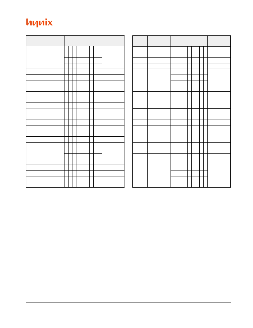
Table 6. Sector Groups - Top Boot Version
Table 7. Sector Groups - Bottom Boot Version
tors can be programmed or erased by invoking
the appropriate commands (see Device Com-
mands section). Once V
ID
is removed from RE-
SET#, all the previously protected sector groups
are protected again. Figure 5 illustrates the algo-
rithm.
NOTE:
If WP#/ACC = V
IL
, the boot sectors remain pro-
tected.
Electronic ID Operation (High Voltage Method)
The Electronic ID mode provides manufacturer
and device identification, sector protection verifi-
cation and Sec
2
region protection status through
identifier codes output on DQ[15:0]. This mode is
intended primarily for programming equipment to
automatically match a device to be programmed
with its corresponding programming algorithm.
Two methods are provided for accessing the Elec-
tronic ID data. The first requires V
ID
on address
pin A[9], with additional requirements for obtain-
相關PDF資料 |
PDF描述 |
|---|---|
| HY29LV320BF-12I | 32 Mbit (2M x 16) Low Voltage Flash Memory |
| HY29LV320TT-90 | 32 Mbit (2M x 16) Low Voltage Flash Memory |
| HY29LV320BT-90 | 32 Mbit (2M x 16) Low Voltage Flash Memory |
| HY29LV320TF-70 | 32 Mbit (2M x 16) Low Voltage Flash Memory |
| HY29LV320TF-80 | 32 Mbit (2M x 16) Low Voltage Flash Memory |
相關代理商/技術參數(shù) |
參數(shù)描述 |
|---|---|
| HY29LV320BF-12I | 制造商:HYNIX 制造商全稱:Hynix Semiconductor 功能描述:32 Mbit (2M x 16) Low Voltage Flash Memory |
| HY29LV320BF-70 | 制造商:HYNIX 制造商全稱:Hynix Semiconductor 功能描述:32 Mbit (2M x 16) Low Voltage Flash Memory |
| HY29LV320BF-70I | 制造商:HYNIX 制造商全稱:Hynix Semiconductor 功能描述:32 Mbit (2M x 16) Low Voltage Flash Memory |
| HY29LV320BF-80 | 制造商:HYNIX 制造商全稱:Hynix Semiconductor 功能描述:32 Mbit (2M x 16) Low Voltage Flash Memory |
| HY29LV320BF-80I | 制造商:HYNIX 制造商全稱:Hynix Semiconductor 功能描述:32 Mbit (2M x 16) Low Voltage Flash Memory |
發(fā)布緊急采購,3分鐘左右您將得到回復。