- 您現(xiàn)在的位置:買賣IC網(wǎng) > PDF目錄384447 > HUF76629D3S (INTERSIL CORP) 20A, 100V, 0.054 Ohm, N-Channel, Logic Level UltraFET Power MOSFET(20A, 100V, 0.054Ω N溝道邏輯電平功率MOS場(chǎng)效應(yīng)管) PDF資料下載
參數(shù)資料
| 型號(hào): | HUF76629D3S |
| 廠商: | INTERSIL CORP |
| 元件分類: | 功率晶體管 |
| 英文描述: | 20A, 100V, 0.054 Ohm, N-Channel, Logic Level UltraFET Power MOSFET(20A, 100V, 0.054Ω N溝道邏輯電平功率MOS場(chǎng)效應(yīng)管) |
| 中文描述: | 20 A, 100 V, 0.055 ohm, N-CHANNEL, Si, POWER, MOSFET, TO-252AA |
| 文件頁(yè)數(shù): | 1/9頁(yè) |
| 文件大小: | 334K |
| 代理商: | HUF76629D3S |
1
File Number
4692.3
CAUTION: These devices are sensitive to electrostatic discharge; follow proper ESD Handling Procedures.
PSPICE is a registered trademark of MicroSim Corporation. UltraFET is a trademark of Intersil Corporation.
SABER
is a Copyright of Analogy, Inc. 1-888-INTERSIL or 407-727-9207
|
Copyright
Intersil Corporation 1999.
HUF76629D3,HUF76629D3S
20A, 100V, 0.054 Ohm, N-Channel, Logic
Level UltraFET Power MOSFET
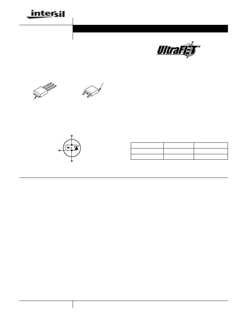
Packaging
JEDEC TO-251AA
Symbol
Features
Ultra Low On-Resistance
- r
DS(ON)
= 0.052
,
V
GS
=
10V
- r
DS(ON)
= 0.054
,
V
GS
=
5V
Simulation Models
- Temperature Compensated PSPICE
and SABER
Electriecal Models
- Spice and SABER Thermal Impedance Models
- www.semi.harris.com
Peak Current vs Pulse Width Curve
UIS Rating Curve
Switching Time vs R
GS
Curves
Ordering Information
Absolute Maximum Ratings
T
C
= 25
o
C, Unless Otherwise Specified
JEDEC TO-252AA
DRAIN
(FLANGE)
GATE
SDRAIN
HUF76629D3
GATE
SOURCE
DRAIN
(FLANGE)
HUF76629D3S
D
G
S
PART NUMBER
PACKAGE
BRAND
HUF76629D3
TO-251AA
76629D
HUF76629D3S
TO-252AA
76629D
NOTE: When ordering, use the entire part number. Add the suffix T
to obtain the variant in tape and reel, e.g., HUF76629D3ST.
HUF76629D3, HUF76629D3S
100
100
±
16
UNITS
V
V
V
Drain to Source Voltage (Note 1). . . . . . . . . . . . . . . . . . . . . . . . . . . . . . . . . . . . . . . . . . V
DSS
Drain to Gate Voltage (R
GS
= 20k
) (Note 1) . . . . . . . . . . . . . . . . . . . . . . . . . . . . . . . .V
DGR
Gate to Source Voltage . . . . . . . . . . . . . . . . . . . . . . . . . . . . . . . . . . . . . . . . . . . . . . . . . . V
GS
Drain Current
Continuous (T
C
= 25
o
C, V
GS
= 5V) . . . . . . . . . . . . . . . . . . . . . . . . . . . . . . . . . . . . . . . . . I
D
Continuous (T
C
= 25
o
C, V
GS
= 10V) (Figure 2) . . . . . . . . . . . . . . . . . . . . . . . . . . . . . . . . I
D
Continuous (T
C
= 100
o
C, V
GS
= 5V) . . . . . . . . . . . . . . . . . . . . . . . . . . . . . . . . . . . . . . . . I
D
Continuous (T
C
= 100
o
C, V
GS
= 4.5V) (Figure 2) . . . . . . . . . . . . . . . . . . . . . . . . . . . . . . I
D
Pulsed Drain Current . . . . . . . . . . . . . . . . . . . . . . . . . . . . . . . . . . . . . . . . . . . . . . . . . . .I
DM
Pulsed Avalanche Rating . . . . . . . . . . . . . . . . . . . . . . . . . . . . . . . . . . . . . . . . . . . . . . . . .UIS
Power Dissipation . . . . . . . . . . . . . . . . . . . . . . . . . . . . . . . . . . . . . . . . . . . . . . . . . . . . . . . P
D
Derate Above 25
o
C . . . . . . . . . . . . . . . . . . . . . . . . . . . . . . . . . . . . . . . . . . . . . . . . . . . . . . .
Operating and Storage Temperature . . . . . . . . . . . . . . . . . . . . . . . . . . . . . . . . . . . . T
J
, T
STG
Maximum Temperature for Soldering
Leads at 0.063in (1.6mm) from Case for 10s. . . . . . . . . . . . . . . . . . . . . . . . . . . . . . . . . .T
L
Package Body for 10s, See Techbrief TB334. . . . . . . . . . . . . . . . . . . . . . . . . . . . . . . . T
pkg
NOTES:
1. T
J
= 25
o
C to 150
o
C.
CAUTION:
Stresses above those listed in “Absolute Maximum Ratings” may cause permanent damage to the device. This is a stress only rating and operation of the
device at these or any other conditions above those indicated in the operational sections of this specification is not implied.
20
20
20
20
Figure 4
A
A
A
A
Figures 6, 17, 18
110
0.74
-55 to 175
W
W/
o
C
o
C
300
260
o
C
o
C
Data Sheet
October 1999
相關(guān)PDF資料 |
PDF描述 |
|---|---|
| HUF76629D3 | Single Supply RS232C Line Driver/Receiver(?????μ?o?RS232C ?o?????????¨???2???2??????) |
| HUF76629D3ST | TRANSISTOR | MOSFET | N-CHANNEL | 100V V(BR)DSS | 20A I(D) | TO-252AA |
| HUF76629D3S | Single Supply RS232C Line Driver/Receiver(?????μ?o?RS232C ?o?????????¨???2???2??????) |
| HUF76639P3 | 50A, 100V, 0.027 Ohm, N-Channel, Logic Level UltraFET Power MOSFET |
| HUF76639P3 | Low Power 5V RS232 Dual Driver/Receiver with 0.1?μF Capacitors; Package: SO; No of Pins: 16; Temperature Range: -40?°C to 85?°C |
相關(guān)代理商/技術(shù)參數(shù) |
參數(shù)描述 |
|---|---|
| HUF76629D3ST | 功能描述:MOSFET 20a 100V 0.054 Ohm Logic Level N-Ch RoHS:否 制造商:STMicroelectronics 晶體管極性:N-Channel 汲極/源極擊穿電壓:650 V 閘/源擊穿電壓:25 V 漏極連續(xù)電流:130 A 電阻汲極/源極 RDS(導(dǎo)通):0.014 Ohms 配置:Single 最大工作溫度: 安裝風(fēng)格:Through Hole 封裝 / 箱體:Max247 封裝:Tube |
| HUF76629D3ST_F085 | 功能描述:MOSFET N-Channel Logic Level UltraFET Power MOSFET 100V, 20A, 52m RoHS:否 制造商:Fairchild Semiconductor 晶體管極性: 汲極/源極擊穿電壓: 閘/源擊穿電壓: 漏極連續(xù)電流: 電阻汲極/源極 RDS(導(dǎo)通): 配置: 最大工作溫度: 安裝風(fēng)格: 封裝 / 箱體: 封裝:Reel |
| HUF76629D3ST_NL | 制造商:Fairchild Semiconductor Corporation 功能描述: |
| HUF76629D3ST_SB82250 | 制造商:Fairchild Semiconductor Corporation 功能描述:FSCHUF76629D3ST_SB82250 ULTRAFET POWER M |
| HUF76629D3STNL | 制造商:Fairchild Semiconductor Corporation 功能描述: |
發(fā)布緊急采購(gòu),3分鐘左右您將得到回復(fù)。