- 您現(xiàn)在的位置:買(mǎi)賣(mài)IC網(wǎng) > PDF目錄370462 > HD404459 (Hitachi,Ltd.) 4-bit HMCS400-Series microcomputer(4位單片微計(jì)算機(jī)) PDF資料下載
參數(shù)資料
| 型號(hào): | HD404459 |
| 廠商: | Hitachi,Ltd. |
| 英文描述: | 4-bit HMCS400-Series microcomputer(4位單片微計(jì)算機(jī)) |
| 中文描述: | 4位HMCS400系列微機(jī)(4位單片微計(jì)算機(jī)) |
| 文件頁(yè)數(shù): | 10/120頁(yè) |
| 文件大?。?/td> | 692K |
| 代理商: | HD404459 |
第1頁(yè)第2頁(yè)第3頁(yè)第4頁(yè)第5頁(yè)第6頁(yè)第7頁(yè)第8頁(yè)第9頁(yè)當(dāng)前第10頁(yè)第11頁(yè)第12頁(yè)第13頁(yè)第14頁(yè)第15頁(yè)第16頁(yè)第17頁(yè)第18頁(yè)第19頁(yè)第20頁(yè)第21頁(yè)第22頁(yè)第23頁(yè)第24頁(yè)第25頁(yè)第26頁(yè)第27頁(yè)第28頁(yè)第29頁(yè)第30頁(yè)第31頁(yè)第32頁(yè)第33頁(yè)第34頁(yè)第35頁(yè)第36頁(yè)第37頁(yè)第38頁(yè)第39頁(yè)第40頁(yè)第41頁(yè)第42頁(yè)第43頁(yè)第44頁(yè)第45頁(yè)第46頁(yè)第47頁(yè)第48頁(yè)第49頁(yè)第50頁(yè)第51頁(yè)第52頁(yè)第53頁(yè)第54頁(yè)第55頁(yè)第56頁(yè)第57頁(yè)第58頁(yè)第59頁(yè)第60頁(yè)第61頁(yè)第62頁(yè)第63頁(yè)第64頁(yè)第65頁(yè)第66頁(yè)第67頁(yè)第68頁(yè)第69頁(yè)第70頁(yè)第71頁(yè)第72頁(yè)第73頁(yè)第74頁(yè)第75頁(yè)第76頁(yè)第77頁(yè)第78頁(yè)第79頁(yè)第80頁(yè)第81頁(yè)第82頁(yè)第83頁(yè)第84頁(yè)第85頁(yè)第86頁(yè)第87頁(yè)第88頁(yè)第89頁(yè)第90頁(yè)第91頁(yè)第92頁(yè)第93頁(yè)第94頁(yè)第95頁(yè)第96頁(yè)第97頁(yè)第98頁(yè)第99頁(yè)第100頁(yè)第101頁(yè)第102頁(yè)第103頁(yè)第104頁(yè)第105頁(yè)第106頁(yè)第107頁(yè)第108頁(yè)第109頁(yè)第110頁(yè)第111頁(yè)第112頁(yè)第113頁(yè)第114頁(yè)第115頁(yè)第116頁(yè)第117頁(yè)第118頁(yè)第119頁(yè)第120頁(yè)
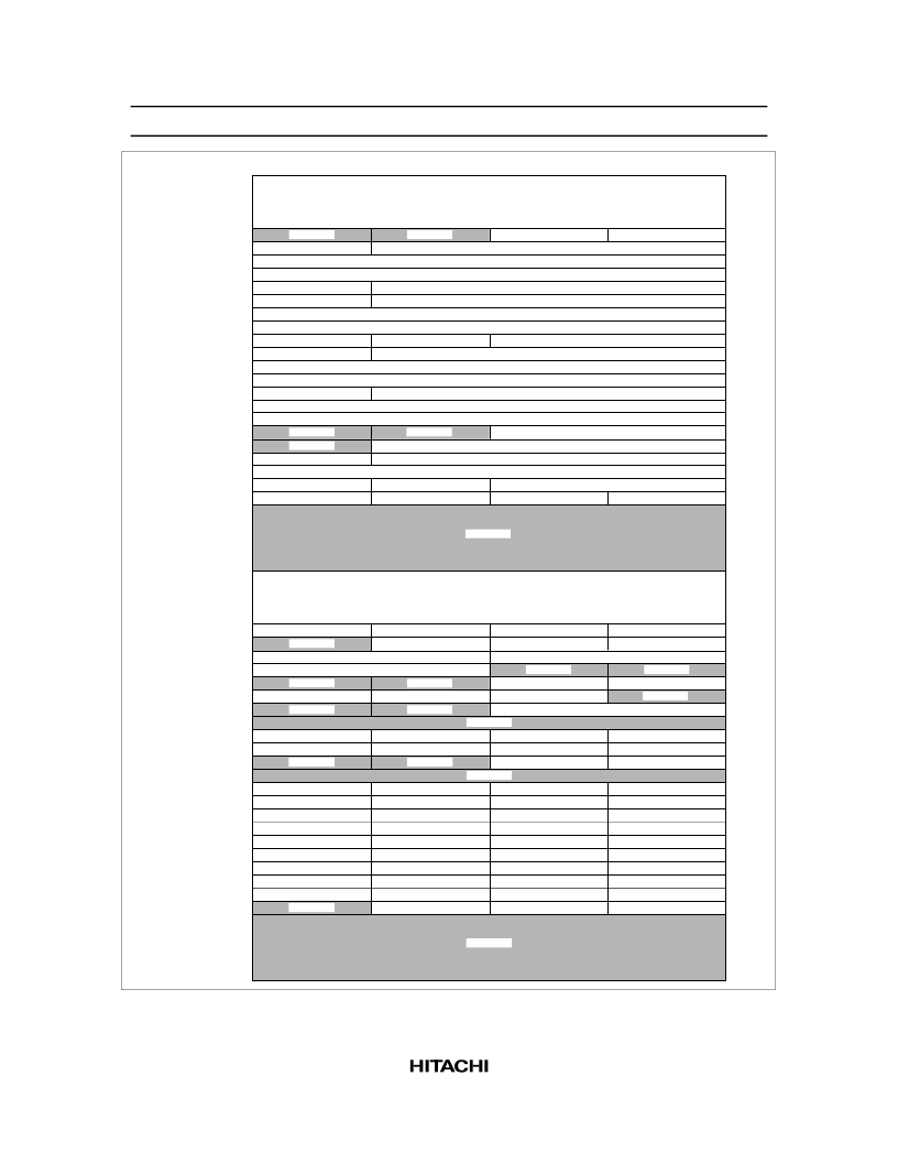
HD404459 Series
10
$000
$003
PMRA $004
SMRA $005
SRL $006
SRU $007
TMA $008
TMB1 $009
TRBL/TWBL $00A
TRBU/TWBU $00B
MIS $00C
TMC1 $00D
TRCL/TWCL$00E
TRCU/TWCU $00F
TMD1 $010
TRDL/TWDL $011
TRDU/TWDU $012
TMB2 $013
TMC2 $014
TMD2 $015
CCR $016
CER $017
WSR $018
$020
$023
PMRB $024
PMRC $025
ESR1 $026
ESR2 $027
SMRB $028
SSR1 $029
SSR2 $02A
DCD0 $02C
DCD1 $02D
DCD2 $02E
DCR0 $030
DCR1 $031
DCR2 $032
DCR3 $033
DCR4 $034
DCR5 $035
DCR6 $036
DCR7 $037
DCR8 $038
DCR9 $039
$03F
Not used
Interrupt control bits area
R4
2
/SI
R4
3
/SO
R4
1
/
SCK
Serial transmit clock speed selection
Serial data register (lower digit)
Serial data register (upper digit)
Clock source selection (timer A)
Clock source selection (timer B)
Timer B register (lower digit)
Timer B register (upper digit)
SO PMOS control
Clock source selection (timer C)
Timer C register (lower digit)
Timer C register (upper digit)
Clock source selection (timer D)
Timer D register (lower digit)
Timer D register (upper digit)
Not used
Timer-A/timer-base
Auto-reload on/off
Pull-up MOS control
Auto-reload on/off
Auto-reload on/off
Interrupt frame period selection
Timer B output mode selection
Timer C output mode selection
Timer D output mode selection
Internal reference voltage level selection
Reference power supply selection
Voltage comparison result
WU
7
WU
6
enable
WU
5
to
WU
4
enable
WU
3
to
WU
0
enable
R0
3
/INT
3
Not used
R0
2
/INT
2
D
11
/
STOPC
R0
1
/
INT
1
R4
0
/EVND
INT
2
detection edge selection
Not used
R0
0
/
INT
0
R3
3
/
EVNB
INT
3
detection edge selection
EVND detection edge selection
Not used
SO output level control in idle states
32-kHz oscillation sampling selection
Serial clock source selection
Not used
32-kHz oscillation stop
Not used
32-kHz oscillation division ratio selection
Not used
OSC division ratio selection
Port D3 DCR
Port D7 DCR
Not used
Port D2 DCR
Port D6 DCR
Not used
Port D1 DCR
Port D5 DCR
Port D9 DCR
Port D0 DCR
Port D4 DCR
Port D8 DCR
Port R0
3
DCR
Port R1
3
DCR
Port R2
3
DCR
Port R3
3
DCR
Port R4
3
DCR
Port R5
3
DCR
Port R6
3
DCR
Port R7
3
DCR
Port R8
3
DCR
Port R0
2
DCR
Port R1
2
DCR
Port R2
2
DCR
Port R3
2
DCR
Port R4
2
DCR
Port R5
2
DCR
Port R6
2
DCR
Port R7
2
DCR
Port R8
2
DCR
Port R9
2
DCR
Port R0
1
DCR
Port R1
1
DCR
Port R2
1
DCR
Port R3
1
DCR
Port R4
1
DCR
Port R5
1
DCR
Port R6
1
DCR
Port R7
1
DCR
Port R8
1
DCR
Port R9
1
DCR
Port R0
0
DCR
Port R1
0
DCR
Port R2
0
DCR
Port R3
0
DCR
Port R4
0
DCR
Port R5
0
DCR
Port R6
0
DCR
Port R7
0
DCR
Port R8
0
DCR
Port R9
0
DCR
Not used
Not used
Not used
Not used
Not used
Not used
Not used
Not used
Not used
Not used
COMP
0
to COMP
3
selection
Register flag area
Bit 3
Bit 2
Bit 1
Bit 0
Input capture selection
Figure 5 Special Function Register Area
相關(guān)PDF資料 |
PDF描述 |
|---|---|
| HD40A4052 | 4-Bit Single-Chip Microcomputer(4位單片微計(jì)算機(jī)) |
| HD404092 | 4-Bit Single-Chip Microcomputer(4位單片微計(jì)算機(jī)) |
| HD404094 | 4-Bit Single-Chip Microcomputer(4位單片微計(jì)算機(jī)) |
| HD4074094 | 4-Bit Single-Chip Microcomputer(4位單片微計(jì)算機(jī)) |
| HD404052 | 4-Bit Single-Chip Microcomputer(4位單片微計(jì)算機(jī)) |
相關(guān)代理商/技術(shù)參數(shù) |
參數(shù)描述 |
|---|---|
| HD404459H | 制造商:RENESAS 制造商全稱(chēng):Renesas Technology Corp 功能描述:4-bit HMCS400-series microcomputers |
| HD404459SERIES | 制造商:未知廠家 制造商全稱(chēng):未知廠家 功能描述: |
| HD404508FS | 制造商:未知廠家 制造商全稱(chēng):未知廠家 功能描述:4-Bit Microcontroller |
| HD404608FS | 制造商:未知廠家 制造商全稱(chēng):未知廠家 功能描述:4-Bit Microcontroller |
| HD404608H | 制造商:未知廠家 制造商全稱(chēng):未知廠家 功能描述:4-Bit Microcontroller |
發(fā)布緊急采購(gòu),3分鐘左右您將得到回復(fù)。